Materials typically conduct electricity or insulate against it—so experimental and theoretical physicists have been captivated by a compound called samarium hexaboride (SmB6) that appears to do both. Numerous studies over the course of 50 years have revealed that SmB6 acts like an insulator as well as an electricity-conducting metal.
Now, researchers from the Harvard John A. Paulson School of Engineering and Applied Sciences (SEAS) say it’s possible to image the exact position of electrons along the surface of SmB6 with single-atom precision, enabling a breakthrough in understanding the compound’s properties and why it can both insulate and conduct. The findings, published in Science, build upon SEAS research reported in 2019 that determined that SmB6 is a topological insulator—meaning it conducts electricity along its surfaces but not its insides.
Despite the 2019 discovery about SmB6‘s surface metallicity, many questions remained about its overall metallicity and why different measurements didn’t generate consistent results.
“Anyone with a voltmeter should be able to tell you whether a material is conductive or insulating,” says Harris Pirie, first author of the paper and a former Ph.D. student in the lab of Clowes Professor of Science Jenny Hoffman at SEAS. But that was never the case with SmB6. “That intrigued us and thrust SmB6 even further into the spotlight within the physics community.
To understand the peculiar behavior of how electrical charges move within SmB6, Pirie and collaborators from University of Oxford, University of Illinois at Chicago (UIC), and other institutions needed to develop a new imaging approach to detect the distribution of electrons on SmB6.
In conversations with Dirk Morr of UIC, the team homed in on the idea of adapting a scanning tunneling microscope, which uses an unimaginably small needle tip to measure atomic structures on the surface of a material. Instead of measuring atomic structure, they used it to detect a magnetic resonance in SmB6 at a cold temperature, a signature of the magnetic interactions that turn the would-be metal into a low-temperature insulator. “That magnetic interaction generates a clear resonance we can measure, and we predicted that if we could measure its excitation energy at different surface points, it would reveal the electronic charge at that position,” Pirie says.
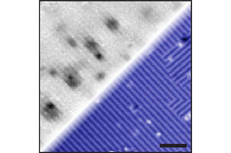
Scanning the needle across the surface of SmB6 to map out the electronic charges across all surface points, the team created a readout that “looks like a topographic map you would have of a mountain range,” Pirie says. Except those mountain peaks and valleys are the size of atoms.
Using this method, the team has captured the first picture of electrons accumulating around atomic defects on SmB6‘s surface—even surfaces created by cross-sectioning a sample of SmB6 into fragments. “It was clear right from the moment we took that measurement, we had found the electrons we were looking for,” Pirie says. “We saw these amazing wave patterns that the electrons formed around the defects, indicating a high signal-to-noise ratio. It was a very cool moment.”
“The work gives us new understanding of the importance of single atom defects in topological materials,” says Hoffman, the paper’s senior author.
Pirie is now looking to modify the scanning tunneling microscope method to build new quantum devices. “The atomic defects we’ve identified could be useful in building quantum circuits. The needle of the scanning tunneling microscope can come so ridiculously close to the sample material that it’s no longer passively imaging it—it can touch and change the sample,” he says. “I’m interested in seeing if we can move atoms around on SmB6, pushing all the electrons into specific, controlled channels or puddles. The hope is that by strategically constructing atomic defects on SmB6, electrons could be precisely trapped to form qubits—the basic units necessary for quantum computing.”
That might help solve a major barrier to a workable quantum computer: to operate stably, the quantum state of a a quantum computer’s qubits must be entirely prohibited from entangling with electrons in the surrounding environment.
The imaging method could give scientists a powerful high-resolution tool to see what electrons are doing on various materials and compounds, Pirie says. “This tool can look at what the electric charge around just one atom is doing—allowing us to see the world at a smaller scale. There are so many fundamental questions this could help us answer about the world around us.”
More information: Harris Pirie et al, Visualizing the atomic-scale origin of metallic behavior in Kondo insulators, Science (2023). DOI: 10.1126/science.abq5375
Journal information: Science
Provided by Harvard John A. Paulson School of Engineering and Applied Sciences

