Miniaturized and multicolored light-emitting device arrays provide a promising instrument to sense, image and compute in materials science and applied physics. A range of emission colors can be achieved by using conventional light emitting diodes, although the process can be limited by material or device constraints.
In a new report published in Science Advances, Vivian Wang and a research team in electrical engineering and materials science at the Lawrence Berkeley National Laboratory, and the University of California, Berkeley, developed a variety of highly multicolored light emitting arrays with diverse colors on a single chip. The array contained pulse-driven metal-oxide-semiconductor capacitors to generate electroluminescence from micro-dispersed materials that spanned a variety of colors and spectral shapes.
The materials scientists and engineers combined compressive reconstruction algorithms to perform spectroscopic measurements in a compact environment, using multiplexed electroluminescent arrays to demonstrate spectral imaging of samples in conjunction with a camera.
Experimental design
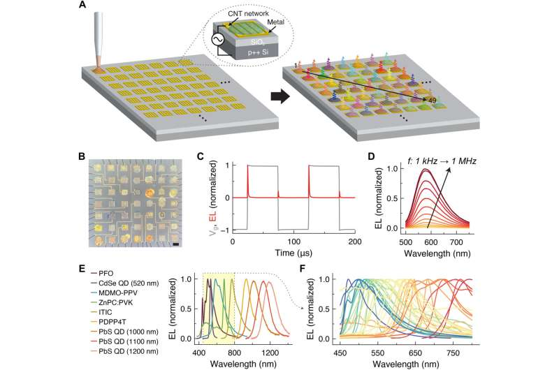
Multicolored light emitting arrays have versatile applications in the field, although the range of colors in use are insufficient for commercial use. In this study, Wang and colleagues addressed the problem by using arrays of electroluminescent, alternating current-driven metal-oxide-semiconductor capacitors, where they lithographically defined the device electrodes prior to depositing the emitting materials. The deposition of the emissive layer formed the final fabrication step in these devices, and the team used microprinting methods to dispense diverse color emitters on a single chip with ease to perform active spectral measurements in a miniaturized environment.

Electroluminescent device arrays with arbitrary spectra
The research team developed multiplexed arrays of light sources via metal-oxide-semiconductor capacitor devices where they deposited emissive materials on top of capacitors engineered on silicon substrates. They applied an alternating current voltage between the two capacitors to overcome differences in band alignment at the metal-semiconductor contact to produce transient electroluminescence during each voltage transition. The materials scientists developed the transient electroluminescence from materials sensitive to the visible to infrared range with variations to both frequency and voltage.
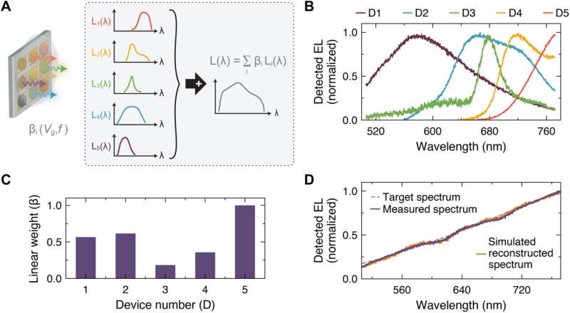
During the experiments, they characterized the brightness, efficiency color and spectral bandwidth of the electroluminescent devices. Due to its simplicity, the team successfully constructed large multicolor electroluminescent arrays on a single substrate. The team accomplished this by developing a 7 x 7 array of light emitting devices, where they deposited a different emissive layer on each pixel via micro-dispersing to obtain a nanometer-thin film. The team highlighted the core characteristics of the device by demonstrating how any light spectra could be generated with a sufficiently large library of emitters. For instance, the total light spectrum from a miniature electroluminescence array facilitated a linear combination of the spectra from individual elements. As a result, the researchers designed an array of emitters to yield a desired light spectrum.

Reconstructive spectral measurement and imaging
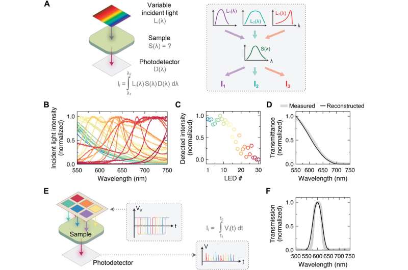
The team showed the scalability and versatility of the device platform alongside the breadth of achievable electroluminescence spectra with active spectral measurements. For example, they measured the transmission spectrum of an unknown sample by passing a broadband light through the sample. In another instance, they measured the spectral information with reconstructive spectrometry to recover spectral information algorithmically. The unique and inherently pulsed nature of the instrument allowed them to conduct alternate spectral measurements and achieve fast spectral measurements without switching devices.
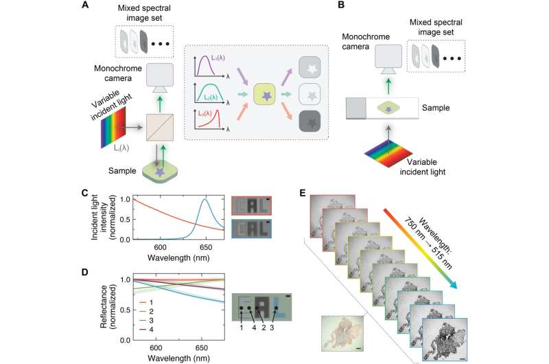
After conducting reconstructive spectral measurements, Wang et al. used the instrument for spectral imaging. In this instance, the electroluminescence arrays served as the light source, while a silicon charge-coupled camera captured images of the samples. They further accomplished spectral imaging of semi-transparent biological samples and maintained the scale of miniaturized light emitting arrays at the nanoscale/microscale on a chip since they can be feasible for a range of adaptive sensing applications.

Outlook
In this way, Vivian Wang and colleagues developed a simple and scalable instrument to house light-emitting device arrays with highly multiplexed emission spanning the visible and infrared wavelengths. The scientists used pulsed-driven metal-oxide semiconductor capacitors to completely integrate the multicolor devices.
This platform is a source of variable light emission via random selection to probe the spectral properties of samples and explore spectral reflectance and transmission imaging. The scientists improved spectral imaging accuracy and coverage with spectrally tuned materials such as colloidal quantum dots and perovskite nanomaterials, or thin luminescent films developed by combinatorial deposition.
This work can be expanded to more extreme wavelengths in addition to the visible spectrum. The pixels in the light emitting arrays can be individually addressed, allowing materials scientists to use the instruments and generate light with customizable patterns in frequency, space and time for multidimensional spectral measurements.
More information: Vivian Wang et al, Highly multicolored light-emitting arrays for compressive spectroscopy, Science Advances (2023). DOI: 10.1126/sciadv.adg1607
Chuan Wang et al, User-interactive electronic skin for instantaneous pressure visualization, Nature Materials (2013). DOI: 10.1038/nmat3711
Journal information: Nature Materials , Science Advances

