The data centers and high-performance computers that run artificial intelligence programs, such as large language models, aren’t limited by the sheer computational power of their individual nodes. It’s another problem—the amount of data they can transfer among the nodes—that underlies the “bandwidth bottleneck” that currently limits the performance and scaling of these systems.
The nodes in these systems can be separated by more than one kilometer. Since metal wires dissipate electrical signals as heat when transferring data at high speeds, these systems transfer data via fiber-optic cables. Unfortunately, a lot of energy is wasted in the process of converting electrical data into optical data (and back again) as signals are sent from one node to another.
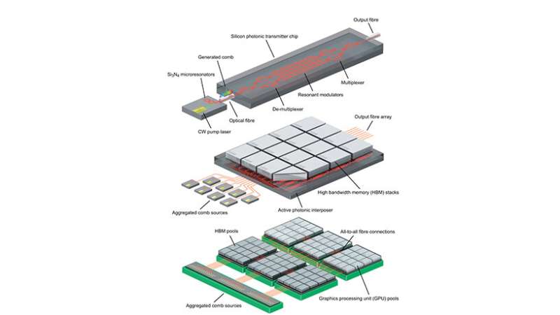
In a study published in Nature Photonics, researchers at Columbia Engineering demonstrate an energy-efficient method for transferring larger quantities of data over the fiber-optic cables that connect the nodes. This new technology improves on previous attempts to transmit multiple signals simultaneously over the same fiber-optic cables. Instead of using a different laser to generate each wavelength of light, the new chips require only a single laser to generate hundreds of distinct wavelengths of light that can simultaneously transfer independent streams of data.
A simpler, more energy-efficient method for data transfer
The millimeter-scale system employs a technique called wavelength-division multiplexing (WDM) and devices called Kerr frequency combs that take a single color of light at the input and create many new colors of light at the output. The critical Kerr frequency combs developed by Michal Lipson, Higgins Professor of Electrical Engineering and Professor of Applied Physics, and Alexander Gaeta, David M. Rickey Professor of Applied Physics and Materials Science and Professor of Electrical Engineering, allowed the researchers to send clear signals through separate and precise wavelengths of light, with space in between them.

“We recognized that these devices make ideal sources for optical communications, where one can encode independent information channels on each color of light and propagate them over a single optical fiber,” says senior author Keren Bergman, Charles Batchelor Professor of Electrical Engineering at Columbia Engineering, where she also serves as the faculty director of the Columbia Nano Initiative. This breakthrough could allow systems to transfer exponentially more data without using proportionately more energy.
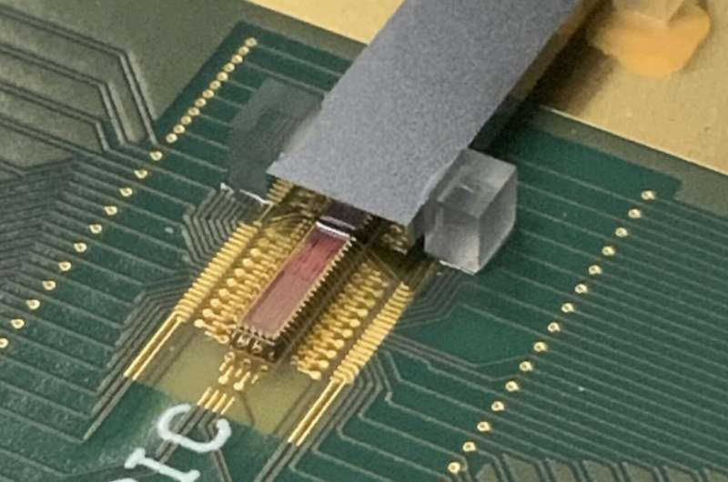
The team miniaturized all of the optical components onto chips roughly a few millimeters on each edge for generating light, encoded them with electrical data, and then converted the optical data back into an electrical signal at the target node. They devised a novel photonic circuit architecture that allows each channel to be individually encoded with data while having minimal interference with neighboring channels. That means the signals sent in each color of light don’t become muddled and difficult for the receiver to interpret and convert back into electronic data.
“In this way, our approach is much more compact and energy-efficient than comparable approaches,” says the study’s lead author Anthony Rizzo, who conducted this work while a Ph.D. student in the Bergman lab and is now a research scientist at the U.S. Air Force Research Laboratory Information Directorate. “It is also cheaper and easier to scale since the silicon nitride comb generation chips can be fabricated in standard CMOS foundries used to fabricate microelectronics chips rather than in expensive dedicated III-V foundries.”
The compact nature of these chips enables them to directly interface with computer electronics chips, greatly reducing the total energy consumption since the electrical data signals only have to propagate over millimeters of distance rather than tens of centimeters.
Bergman noted, “What this work shows is a viable path towards both dramatically reducing the system energy consumption while simultaneously increasing the computing power by orders of magnitude, allowing artificial intelligence applications to continue to grow at an exponential rate with minimal environmental impact.”
Exciting results pave the way to real-world deployment
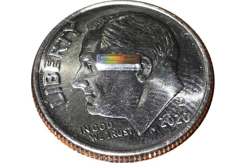
In experiments, the researchers managed to transmit 16 gigabits per second per wavelength for 32 distinct wavelengths of light for a total single-fiber bandwidth of 512 Gb/s with less than one bit in error out of one trillion transmitted bits of data. These are incredibly high levels of speed and efficiency. The silicon chip transmitting the data measured just 4mm x 1mm, while the chip that received the optical signal and converted it into an electrical signal measured just 3mm x 1mm—both smaller than a human fingernail.

“While we used 32 wavelength channels in the proof-of-principle demonstration, our architecture can be scaled to accommodate over 100 channels, which is well within the reach of standard Kerr comb designs,” Rizzo adds.
These chips can be fabricated using the same facilities used to make the microelectronics chips found in a standard consumer laptop or cellphone, providing a straightforward path to volume scaling and real-world deployment.
The next step in this research is to integrate the photonics with chip-scale driving and control electronics to further miniaturize the system.
More information: Massively scalable Kerr comb-driven silicon photonic link, Nature Photonics (2023). DOI: 10.1038/s41566-023-01244-7 , www.nature.com/articles/s41566-023-01244-7
Journal information: Nature Photonics
Provided by Columbia University School of Engineering and Applied Science

