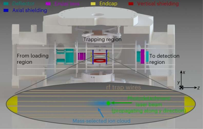
Experimental setup and thermalization dynamics under position-dependent photodetachment. Credit: Nature Physics (2023). DOI: 10.1038/s41567-023-02084-6
A team of physicists at the Physikalisches Institut, Ruprecht-Karls-Universität working with colleagues from Institut für Ionenphysik und Angewandte Physik, Universität Innsbruck, has developed a laser technique to selectively remove the most energetic ions from a sample, cooling those that remain.
In their paper published in the journal Nature Physics, the group describes their method and possible uses for it. The team at Nature has also published a Research Highlights paper in the same issue outlining the work by the team on this new effort.
Cooling molecular ions is useful in a wide variety of applications in both physics and chemistry research, including current work to better understand the chemistry of celestial bodies such as Saturn’s moon Titan. Unfortunately, cooling negatively charged molecules has proven to be more difficult, and their use has been limited. In this new effort, the research team developed a technique that makes the process relatively easy.
The idea stems from prior work involving the use of evaporative cooling, a technology related to evaporative coolers that are used to cool homes in dry areas. In this instance, the technology was used to negatively charge antiprotons by changing the shape of the trap containing them.
In this new work, the team started by using a radio frequency trap to hold a sample of OH– anions at approximately 370 K. They used a special type of laser known as a single photo-detachment laser to manipulate the anions in the trap. This was done by tuning the laser to a desired threshold, which neutralized ions crossing the laser beam, allowing them to be removed from the trap.
As this process continued, those anions with the highest energies were slowly removed, leaving those with lower energies behind. And that left the entire trap and the remaining sample much cooler. In subsequent trials, the team found that they were able to optimize the process, resulting in cooling the trap by several orders of magnitude.
The team concludes that their technique could be used in lab studies and also with research related to better understanding interstellar clouds or the atmosphere of celestial bodies such as Titan.
More information: Jonas Tauch et al, Laser-induced forced evaporative cooling of molecular anions below 4 K, Nature Physics (2023). DOI: 10.1038/s41567-023-02084-6
Photonic integrated link driven by Kerr frequency comb. Credit: The Lightwave Research Laboratory/Columbia Engineering
The data centers and high-performance computers that run artificial intelligence programs, such as large language models, aren’t limited by the sheer computational power of their individual nodes. It’s another problem—the amount of data they can transfer among the nodes—that underlies the “bandwidth bottleneck” that currently limits the performance and scaling of these systems.
The nodes in these systems can be separated by more than one kilometer. Since metal wires dissipate electrical signals as heat when transferring data at high speeds, these systems transfer data via fiber-optic cables. Unfortunately, a lot of energy is wasted in the process of converting electrical data into optical data (and back again) as signals are sent from one node to another.
In a study published in Nature Photonics, researchers at Columbia Engineering demonstrate an energy-efficient method for transferring larger quantities of data over the fiber-optic cables that connect the nodes. This new technology improves on previous attempts to transmit multiple signals simultaneously over the same fiber-optic cables. Instead of using a different laser to generate each wavelength of light, the new chips require only a single laser to generate hundreds of distinct wavelengths of light that can simultaneously transfer independent streams of data.
A simpler, more energy-efficient method for data transfer
The millimeter-scale system employs a technique called wavelength-division multiplexing (WDM) and devices called Kerr frequency combs that take a single color of light at the input and create many new colors of light at the output. The critical Kerr frequency combs developed by Michal Lipson, Higgins Professor of Electrical Engineering and Professor of Applied Physics, and Alexander Gaeta, David M. Rickey Professor of Applied Physics and Materials Science and Professor of Electrical Engineering, allowed the researchers to send clear signals through separate and precise wavelengths of light, with space in between them.
Photonic Integrated Chip placed on a dime. Credit: Lightwave Research Laboratory/Columbia Engineering
“We recognized that these devices make ideal sources for optical communications, where one can encode independent information channels on each color of light and propagate them over a single optical fiber,” says senior author Keren Bergman, Charles Batchelor Professor of Electrical Engineering at Columbia Engineering, where she also serves as the faculty director of the Columbia Nano Initiative. This breakthrough could allow systems to transfer exponentially more data without using proportionately more energy.
The team miniaturized all of the optical components onto chips roughly a few millimeters on each edge for generating light, encoded them with electrical data, and then converted the optical data back into an electrical signal at the target node. They devised a novel photonic circuit architecture that allows each channel to be individually encoded with data while having minimal interference with neighboring channels. That means the signals sent in each color of light don’t become muddled and difficult for the receiver to interpret and convert back into electronic data.
“In this way, our approach is much more compact and energy-efficient than comparable approaches,” says the study’s lead author Anthony Rizzo, who conducted this work while a Ph.D. student in the Bergman lab and is now a research scientist at the U.S. Air Force Research Laboratory Information Directorate. “It is also cheaper and easier to scale since the silicon nitride comb generation chips can be fabricated in standard CMOS foundries used to fabricate microelectronics chips rather than in expensive dedicated III-V foundries.”
The compact nature of these chips enables them to directly interface with computer electronics chips, greatly reducing the total energy consumption since the electrical data signals only have to propagate over millimeters of distance rather than tens of centimeters.
Bergman noted, “What this work shows is a viable path towards both dramatically reducing the system energy consumption while simultaneously increasing the computing power by orders of magnitude, allowing artificial intelligence applications to continue to grow at an exponential rate with minimal environmental impact.”
Exciting results pave the way to real-world deployment
In experiments, the researchers managed to transmit 16 gigabits per second per wavelength for 32 distinct wavelengths of light for a total single-fiber bandwidth of 512 Gb/s with less than one bit in error out of one trillion transmitted bits of data. These are incredibly high levels of speed and efficiency. The silicon chip transmitting the data measured just 4mm x 1mm, while the chip that received the optical signal and converted it into an electrical signal measured just 3mm x 1mm—both smaller than a human fingernail.
Illustration of a disaggregated data center based on Kerr frequency comb-driven silicon photonic links. Credit: Lightwave Research Laboratory/Columbia Engineering
“While we used 32 wavelength channels in the proof-of-principle demonstration, our architecture can be scaled to accommodate over 100 channels, which is well within the reach of standard Kerr comb designs,” Rizzo adds.
These chips can be fabricated using the same facilities used to make the microelectronics chips found in a standard consumer laptop or cellphone, providing a straightforward path to volume scaling and real-world deployment.
The next step in this research is to integrate the photonics with chip-scale driving and control electronics to further miniaturize the system.
Researchers used extremely short laser pulses to make their Q-silicon discovery. Credit: Materials Research Letters (2023). DOI: 10.1080/21663831.2023.2224396
Researchers at North Carolina State University have discovered a new distinct form of silicon called Q-silicon which, among other interesting properties, is ferromagnetic at room temperature. The findings could lead to advances in quantum computing, including the creation of a spin qubit quantum computer that is based on controlling the spin of an electron.
“The discovery of Q-silicon having robust room temperature ferromagnetism will open a new frontier in atomic-scale, spin-based devices and functional integration with nanoelectronics,” said Jay Narayan, the John C. Fan Family Distinguished Chair in Materials Science and corresponding author of a paper describing the work published in Materials Research Letters.
Ferromagnetism in materials outside of transition metals and rare earths has excited scientists worldwide for a long time. This is because spin-polarized electrons can be used to process and store information with atomic resolution. However, materials with even numbers of electrons, such as carbon and silicon, without unpaired spins were not considered seriously in terms of bulk ferromagnetism. The dangling bonds in bulk carbon and silicon materials usually reconstruct and eliminate sources of unpaired electrons.
The NC State researchers showed that laser melting and quenching silicon can result in the formation of Q-silicon. The entire process is completed in less than a fraction of a microsecond, or millionth of a second. Narayan pioneered the use of lasers to create new materials with novel properties in work spanning more than four decades.
Besides ferromagnetism, other Q-silicon properties of interest include enhanced hardness and superconductivity, Narayan says.
“This discovery of Q-silicon stands to revolutionize modern microelectronics by adding new functionalities, such as spintronics, or spin-based quantum computing,” Narayan said. “Modern microelectronics is based upon the charge of an electron, making them relatively slow with limited mobility. By using Q-silicon, we make use of the spin of the electron, making computers much faster with negligible power consumption.
“In short, Q-silicon provides an ideal platform for integration of spintronics with microelectronics on a chip,” said Narayan.
More information: Jagdish Narayan et al, Synthesis and novel properties of Q-silicon (January 2023), Materials Research Letters (2023). DOI: 10.1080/21663831.2023.2224396
Optical micrograph of the electro-optic isolator chip on thin-film lithium niobate, comprising four devices with varying modulation length. Credit: Loncar Lab/Harvard SEAS
An optical isolator developed at the Harvard John A. Paulson School of Engineering and Applied Sciences (SEAS) could drastically improve optical systems for many practical applications.
All optical systems—used for telecommunications, microscopy, imaging, quantum photonics, and more—rely on a laser to generate photons and beams of light. To prevent those lasers from damage and instability, these systems also require isolators, components that prevent light from traveling in undesired directions. Isolators also help cut down on signal noise by preventing light from bouncing around unfettered. But conventional isolators have been relatively bulky in size and require more than one type of material to be joined together, creating a roadblock to achieving enhanced performance.
Now, a team of researchers led by electrical engineer Marko Lončar at SEAS has developed a method for building a highly-efficient integrated isolator that’s seamlessly incorporated into an optical chip made of lithium niobate. Their findings are reported in Nature Photonics.
“We constructed a device that lets light emitted by the laser propagate unaltered, while the reflected light that travels back towards the laser changes its color and gets re-routed away from the laser,” said Lončar, Tiantsai Lin Professor of Electrical Engineering at SEAS. “This is accomplished by sending electrical signals in the direction of the reflected optical signals, thus taking advantage of the excellent electro-optic properties of lithium niobate,” in which voltage can be applied to change the properties of optical signals, including speed and color.
“We wanted to create a safer environment for a laser to operate in, and by designing this one-way street for light, we can protect the device from the laser’s reflection,” said Mengjie Yu, co-first author on the paper and a former postdoctoral researcher in Lončar’s lab. “To our knowledge, when compared to all other demonstrations of integrated isolators, this device performs the best optical isolation in the world. In addition to isolation, it offers the most competitive performance across all metrics including loss, power efficiency, and tunability.”
“What’s exceptional about this device is that at its core it’s incredibly simple—it’s really just one single modulator,” says Rebecca Cheng, co-first author on the paper and a current Ph.D. student in Lončar’s lab. “All previous attempts at engineering something like this required multiple resonators and modulators. The reason we can do this with such remarkable performance is because of lithium niobate’s properties.”
Another reason for the high performance and efficiency has to do with the size of the device—the team built it at the Harvard Center for Nanoscale Systems, fabricating a chip measuring 600 nanometers thick with etchings (to guide the light using prescribed nanostructures) up to 320 nanometers deep.
“With a smaller device, you can control light more easily and also put that light in closer proximity to the electrical signals, thus achieving a stronger electrical field with the same voltage,” enabling more powerful control of light, Yu said.
The scaled-down dimensions and ultralow loss property of this platform also boost optical power. “Since the light doesn’t have to travel so far, there is less decay and loss of power,” Cheng said.
Finally, the teams show the device can successfully protect an on-chip laser from external reflection. “We are the first team to show the laser’s phase-stable operation under the protection of our optical isolator,” said Yu.
Altogether, the advance represents a significant leap forward for practical, high-performance optical chips. The team reports that it can be used with a range of laser wavelengths, only requiring a counter-propagating electrical signal to achieve the desired effects.
The team hopes the breakthrough—part of a larger effort to integrate lasers and photonics components on a chip at extremely small scales—will unlock new capabilities in a range of applications, spanning the telecommunications industry to time-frequency transfer, a way of precisely measuring time down to the atomic and sub-atomic scale that could have implications for quantum research and computing.
“Integrating all aspects of an optical system onto a single chip could replace many larger, more costly, and less efficient systems,” Yu said. “Combining all these things could revolutionize many fields of work.”
More information: Mengjie Yu et al, Integrated electro-optic isolator on thin-film lithium niobate, Nature Photonics (2023). DOI: 10.1038/s41566-023-01227-8
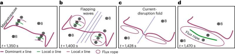
Simplified schematics showing the events within the tail current sheet leading to the eruption of the tail-wide plasmoid. a, The situation within Fig. 1b, showing the two local reconnection regions Earthward and tailward of the dominant x line. Magnetic field topology is given, with ⊙ and ⊗ symbols representing outward and inward directions with respect to the plane and corresponding to Bz > 0 and Bz < 0, respectively. b, The situation within Fig. 1c, where the dusk flank local flux rope is mainly Earthward of the dominant x line. The flapping begins. c, The situation within Fig. 1d, where the flapping waves have evolved into the strong central fold in the noon–midnight meridional plane. The flux ropes have grown and moved tailwards and towards the center of the plasma sheet. d, The situation within Fig. 1g, where the large tail-wide plasmoid has been formed from the two local flank flux ropes. Their merging in the center current sheet was enabled by the current disruption within the central fold. In all panels, the position of the dominant x line is a result of a competition between two x lines. The one that is stronger diverts flow, and hence the global flow reversal changes position. Credit: Nature Geoscience (2023). DOI: 10.1038/s41561-023-01206-2. https://www.nature.com/articles/s41561-023-01206-2
How are plasma eruptions in near-Earth space formed? Vlasiator, a model designed at the University of Helsinki for simulating near-Earth space, demonstrated that the two central theories on the occurrence of eruptions are simultaneously valid: eruptions are explained by both magnetic reconnection and kinetic instabilities.
Rapid plasma eruptions known as plasmoids take place on the nightside of the magnetosphere. Plasmoids are also associated with the sudden brightening of the aurora. The space physics research group at the University of Helsinki investigates and simulates these difficult-to-predict eruptions in near-Earth space using the Vlasiator model.
“The phenomena associated with plasmoids cause the most intense but the least predictable magnetic disturbances, which can cause, for example, disturbances in electrical grids,” says Professor of Computational Space Physics Minna Palmroth from the University of Helsinki. “These eruptions occur on a daily basis, in varying sizes, in the ‘tail’ of the magnetosphere.”
Palmroth is also the director of the Center of Excellence in Research of Sustainable Space, and the principal investigator for the Vlasiator simulation.
“The chain of events leading to plasmoids is one of the longest-standing unresolved questions in space physics: solutions have been sought for it since the 1960s,” Palmroth says.
Near-Earth space is a unique place for understanding plasma eruptions
Two competing lines of thinking have been proposed to explain the course of events, the first asserting that magnetic reconnection severs a part of the magnetotail into a plasmoid. According to the other explanation, kinetic instabilities disrupt the current sheet (a wide, thin distribution of electric current) maintaining the tail, which eventually results in the ejection of a plasmoid. Arguments about the primacy of these two phenomena have been ongoing for decades.
“It now appears that the causalities are in fact more complex than previously understood,” Palmroth says.
The Vlasiator simulation, which requires the processing power of a supercomputer, modeled near-Earth space for the first time in six dimensions and on a scale corresponding to the size of the magnetosphere. The 6D modeling was successful in describing the physics phenomena underlying both paradigms.
“It was a difficult technical challenge that no one else has been able to model,” Palmroth says. Behind the achievement is more than 10 years of software development.
Consequently, the study was able to demonstrate that both magnetic reconnection and kinetic instabilities explain the functioning of the magnetotail. The phenomena associated with these seemingly contradictory theories actually both take place, and simultaneously.
The finding helps to understand how plasma eruptions can occur. This helps in designing spacecraft and equipment, observing these events for further research, and improving the predictability of space weather by improving the understanding of near-Earth space.
The paper is published in the journal Nature Geoscience.
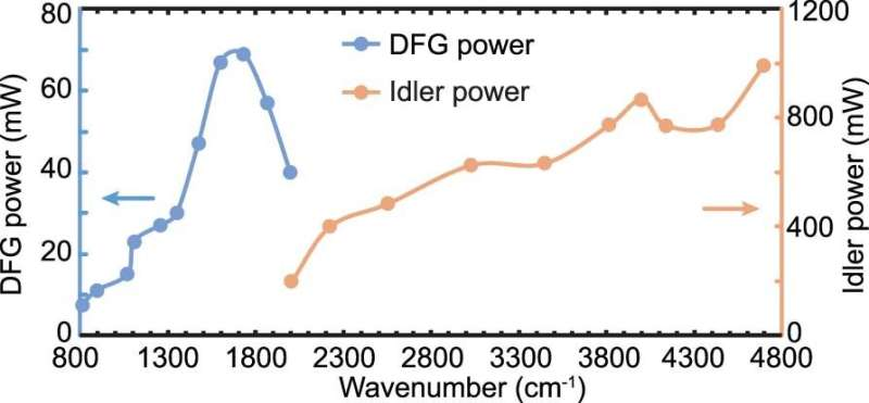
Power outputs of the Idler and the DFG IR lasers. The power is measured at the laser outputs using a thermopile power meter (919P-003-10, Newport). All wavenumbers between 800 and 4800 cm−1 (2.1–12 μm) are covered. The pulse width is 2 ps with a bandwidth of 8–10 cm−1 according to the manufacturer (APE Angewandte Physik & Elektronik GmbH, Berlin, Germany). Credit: Nature Photonics (2023). DOI: 10.1038/s41566-023-01243-8
If you imagine yourself peering through a microscope, you probably picture looking at a glass slide with an amoeba, or maybe a human cell, or perhaps even a small insect of some kind.
But microscopes can see much more than these small living things, and a new type of microscopy developed at Caltech is making it easier to see the very molecules that make up living things.
In a paper appearing in the journal Nature Photonics, researchers from the lab of Lu Wei, assistant professor of chemistry and investigator with the Heritage Medical Research Institute, demonstrate what they are calling bond-selective fluorescence-detected infrared-excited spectro-microscopy, or BonFIRE.
BonFIRE combines two microscopy techniques into one process with greater selectivity and sensitivity, enabling researchers to visualize biological processes at the unprecedented single-molecule level and understand biological mechanisms from a molecular point of view.
“With our new microscope, we can now visualize single molecules with vibrational contrast, which is challenging to do with existing technologies.” says Dongkwan Lee, study co-author and chemical engineering graduate student.
One technique involved in BonFIRE is fluorescence microscopy, which images molecules and other microscopic structures by tagging them with fluorescent chemical markers, causing them to glow when imaged.
Postodoctoral scholar Haomin Wang (left) and graduate student Dongkwan Lee (right) demonstrate operation of the BonFIRE microscopy apparatus. Credit: Caltech
The other technique is vibrational microscopy, which makes use of natural vibrations in the bonds that hold together the atoms of a molecule. A sample to be imaged is bombarded with light, in this case infrared light. That bombardment causes the bonds of the material’s molecules to vibrate in such a way that their type can be identified. Vibrations of a triple bond will “sound” different than the vibrations of a single bond, and the vibrations of a carbon atom bonded to another carbon atom will sound different than the vibrations of a carbon atom bonded to a nitrogen atom, for example. It’s not unlike how a trained guitarist would be able to tell which string on a guitar was plucked and what material it is made from just by listening to the tone it makes.
Wei says that fluorescence microscopy allows researchers to observe single molecules, but it does not provide rich chemical information. On the other hand, vibrational microscopy provides that rich chemical information but only works when the molecule being imaged is present in large amounts.
BonFIRE gets around these limitations by coupling vibrations to fluorescence, effectively combining the strengths of the two techniques. The process works like this: The sample is first stained with a fluorescent dye that bonds to the molecules intended to be imaged. The sample is then bombarded by a pulse of infrared light, whose frequency is tuned to excite a specific bond found in that dye. Once the bond is excited by just a single photon of that light, a second higher-energy pulse of light shines on it and excites it to fluoresce with a glow that can be detected by the microscope. In this way, the microscope can image entire cells or single molecules.
“We are fascinated by this spectroscopy process and are excited to turn it into a novel tool for modern bioimaging,” says Haomin Wang, study co-author and postdoctoral scholar research associate in chemistry. “Over the past three years, we have been on an adventure to build our custom BonFIRE microscope and gain deeper understanding on this spectroscopic process, which further helped us to optimize each component in our setup to reach the performance we have now.”
In their paper, the researchers also demonstrate the ability to tag biomolecules with “colors,” allowing them to be differentiated from each other. This is done by using several isotopes of the atoms that make up the dye molecule. (Isotopes are forms of an element with different atomic weights because their nuclei have greater or fewer neutrons). The frequency at which their bonds vibrate changes with the increased or decreased mass of the atoms.
“Unlike conventional fluorescence microscopy, which can only distinguish a handful of colors at a time, BonFIRE uses infrared light to excite different chemical bonds and produces a rainbow of vibrational colors,” Wei says. “You can label and image many different targets from the same sample at a time and reveal the molecular diversity of life in stunning detail. We hope to be able to demonstrate the imaging capability with tens of colors in live cells in the near future.”
Additional co-authors are chemistry graduate students Yulu Cao, Xiaotian Bi, Jiajun Du, and Kun Miao.
More information: Haomin Wang et al, Bond-selective fluorescence imaging with single-molecule sensitivity, Nature Photonics (2023). DOI: 10.1038/s41566-023-01243-8
In dense nuclear matter, quarks “line up,” becoming essentially one-dimensional. Calculations considering that single dimension plus time can track how low energy excitations ripple through nuclear matter. Credit: Brookhaven National Laboratory
Understanding the behavior of nuclear matter—including the quarks and gluons that make up the protons and neutrons of atomic nuclei—is extremely complicated. This is particularly true in our world, which is three dimensional. Mathematical techniques from condensed matter physics that consider interactions in just one spatial dimension (plus time) greatly simplify the challenge.
Using this two-dimensional approach, scientists solved the complex equations that describe how low-energy excitations ripple through a system of dense nuclear matter. This work indicates that the center of neutron stars, where such dense nuclear matter exists in nature, may be described by an unexpected form.
Being able to understand the quark interactions in two dimensions opens a new window into understanding neutron stars, the densest form of matter in the universe. The approach could help advance the current “golden age” for studying these exotic stars. This surge in research success was triggered by recent discoveries of gravitational waves and electromagnetic emissions in the cosmos.
This work shows that for low-energy excitations, all of the complications of the three-dimensional quark interactions fall away. These low-energy excitations are slight disturbances triggered as a neutron star emits radiation or by its own spinning magnetic fields. This approach might also enable new comparisons with quark interactions in less dense but much hotter nuclear matter generated in heavy-ion collisions.
The modern theory of nuclei, known as quantum chromodynamics, involves quarks bound by the strong nuclear force. This force, carried by gluons, confines quarks into nucleons (protons and neutrons).
When the density of nuclear matter increases, as it does inside neutron stars, the dense system behaves more like a mass of quarks, without sharp boundaries between individual nucleons. In this state, quarks at the edge of the system are still confined by the strong force, as quarks on one side of the spherical system interact strongly with quarks on the opposite side.
This work by researchers at Brookhaven National Laboratory uses the one-dimensional nature of this strong interaction, plus the dimension of time, to solve for the behavior of excitations with low energy near the edge of the system. These low energy modes are just like those of a free, massless boson—which is known in condensed matter as a “Luttinger liquid.”
This method allows scientists to compute the parameters of a Luttinger liquid at any given density. It will advance their ability to explore qualitatively new phenomena expected to occur at the extreme densities within neutron stars, where nuclear matter behaves quite differently than it does in ordinary nuclei, and compare it with much hotter (trillion-degree) dense nuclear matter generated in heavy-ion collisions.
The work is published in the journal Physical Review D.
More information: Marton Lajer et al, When cold, dense quarks in 1+1 and 3+1 dimensions are not a Fermi liquid, Physical Review D (2022). DOI: 10.1103/PhysRevD.105.054035
AI, machine learning, and ChatGPT may be relatively new buzzwords in the public domain, but developing a computer that functions like the human brain and nervous system—both hardware and software combined—has been a decades-long challenge. Engineers at the University of Pittsburgh are today exploring how optical “memristors” may be a key to developing neuromorphic computing.
Resistors with memory, or memristors, have already demonstrated their versatility in electronics, with applications as computational circuit elements in neuromorphic computing and compact memory elements in high-density data storage. Their unique design has paved the way for in-memory computing and captured significant interest from scientists and engineers alike.
A new review article published in Nature Photonics, titled “Integrated Optical Memristors,” sheds light on the evolution of this technology—and the work that still needs to be done for it to reach its full potential.
Led by Nathan Youngblood, assistant professor of electrical and computer engineering at the University of Pittsburgh Swanson School of Engineering, the article explores the potential of optical devices which are analogs of electronic memristors. This new class of device could play a major role in revolutionizing high-bandwidth neuromorphic computing, machine learning hardware, and artificial intelligence in the optical domain.
“Researchers are truly captivated by optical memristors because of their incredible potential in high-bandwidth neuromorphic computing, machine learning hardware, and artificial intelligence,” explained Youngblood. “Imagine merging the incredible advantages of optics with local information processing. It’s like opening the door to a whole new realm of technological possibilities that were previously unimaginable.”
The review article presents a comprehensive overview of recent progress in this emerging field of photonic integrated circuits. It explores the current state-of-the-art and highlights the potential applications of optical memristors, which combine the benefits of ultrafast, high-bandwidth optical communication with local information processing. However, scalability emerged as the most pressing issue that future research should address.
“Scaling up in-memory or neuromorphic computing in the optical domain is a huge challenge. Having a technology that is fast, compact, and efficient makes scaling more achievable and would represent a huge step forward,” explained Youngblood.
“One example of the limitations is that if you were to take phase change materials, which currently have the highest storage density for optical memory, and try to implement a relatively simplistic neural network on-chip, it would take a wafer the size of a laptop to fit all the memory cells needed,” he continued. “Size matters for photonics, and we need to find a way to improve the storage density, energy efficiency, and programming speed to do useful computing at useful scales.”
Using light to revolutionize computing
Optical memristors can revolutionize computing and information processing across several applications. They can enable active trimming of photonic integrated circuits (PICs), allowing for on-chip optical systems to be adjusted and reprogrammed as needed without continuously consuming power. They also offer high-speed data storage and retrieval, promising to accelerate processing, reduce energy consumption, and enable parallel processing.
Optical memristors can even be used for artificial synapses and brain-inspired architectures. Dynamic memristors with nonvolatile storage and nonlinear output replicate the long-term plasticity of synapses in the brain and pave the way for spiking integrate-and-fire computing architectures.
Research to scale up and improve optical memristor technology could unlock unprecedented possibilities for high-bandwidth neuromorphic computing, machine learning hardware, and artificial intelligence.
“We looked at a lot of different technologies. The thing we noticed is that we’re still far away from the target of an ideal optical memristor–something that is compact, efficient, fast, and changes the optical properties in a significant manner,” Youngblood said. “We’re still searching for a material or a device that actually meets all these criteria in a single technology in order for it to drive the field forward.”
More information: Nathan Youngblood et al, Integrated optical memristors, Nature Photonics (2023). DOI: 10.1038/s41566-023-01217-w
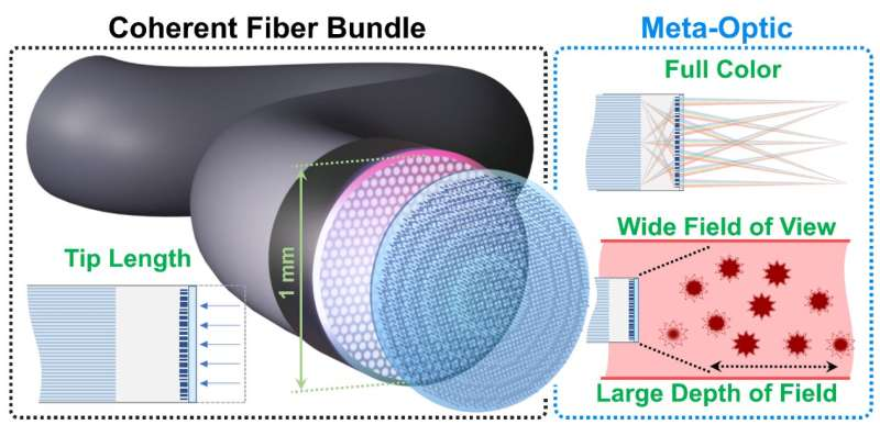
A meta-optic is optimized for integration with the coherent fiber bundle, whereas the individual fiber cores are taken as the imaging limitation. The MOFIE achieves a reduced tip length while maintaining a wide field of view of 22.5° and a large depth of field exceeding 30 mm, compared with a traditional GRIN lens. Credit: Johannes E. Fröch, Luocheng Huang, Quentin A.A. Tanguy, Shane Colburn, Alan Zhan, Andrea Ravagli, Eric J. Seibel, Karl Böhringer, Arka Majumdar
Ultra-compact, agile endoscopes with a large field of view (FoV), long depth of field (DoF), and short rigid tip length are essential for developing minimally invasive operations and new experimental surgeries. As these fields develop, the requirement for miniaturization and increased precision become progressively demanding.
In existing endoscopes, the rigid tip length is a fundamental limitation of the device’s agility within small tortuous ducts, such as an artery. It is primarily constrained by the size of the optical elements required for imaging. Thus, alternative solutions are urgently needed to reduce the tip length.
In a new paper published in eLight, a team of scientists led by Dr. Johannes Fröch and Prof Arka Majumdar from the University of Washington have developed a novel technique for reducing the rigid tip length.
Existing solutions include lensless and computational imaging with single fibers or coherent fiber bundles. However, these are typically limited to a short working distance and often extremely sensitive to bending and twisting of the optical fiber, affecting or even precluding accurate computational reconstruction.
Flat meta-optics are an emerging and versatile idea in the photonics community to create miniaturized optical elements. These are sub-wavelength diffractive optical elements composed of nano-scale scatterer arrays. They are designed to shape an incident wavefront’s phase, amplitude, and spectral response. Such ultrathin flat optics not only dramatically shrink the size of traditional optics but can also combine multiple functionalities in a single surface.
Flat meta-optics are compatible with high-volume semiconductor manufacturing technology and can create disposable optics. These properties have already inspired researchers to explore the potential of meta-optics for endoscopy, including fiber-integrated endoscopy, side-viewing single fiber scanning endoscopy, and scanning fiber forward-viewing endoscopy.
An optical microscope image of the fabricated meta-optic(left ) placed in front of the coherent fiber bundle. Scanning electron microscope imagesof the meta-optic (right) show the individual scatterer, which spans the entire aperture of the device. Credit: Johannes E. Fröch, Luocheng Huang, Quentin A.A. Tanguy, Shane Colburn, Alan Zhan, Andrea Ravagli, Eric J. Seibel, Karl Böhringer, Arka Majumdar
Unfortunately, meta-optics traditionally suffer from strong aberrations, making large FoV and full-color imaging challenging. Several works have shown that the standard metalens design is unsuitable for simultaneously capturing color information across the visible spectrum.
It typically results in crisp images for the design wavelength (e.g. green) but strongly aberrated/ blurred for other colors (red and blue). While some approaches like dispersion engineering and computational imaging techniques can reduce chromatic aberration, they either suffer from small apertures, low numerical apertures or require a computational post-processing step, complicating real-time video capture.
Similarly, an additional aperture before the meta-optic can provide a larger FoV. However, it comes at the cost of reduced light collection and increased thickness of the optics. So far, these limitations have restricted most meta-optics endoscopes to single wavelength operation.
Although, recently, a meta-optic doublet was demonstrated in conjunction with a coherent fiber bundle for polychromatic imaging. Such polychromatic imaging is unsuitable for broad-band illumination, which is often the case for clinical endoscopy. Additionally, the front aperture was limited to 125 μm, with a short working distance of 200 μm.
The research team noted a desire for broad-band, ultra-thin meta-optics for endoscopy. However, making it smaller than the optical fiber diameter is not conducive and severely limits the light collection. As such, full-color meta-optical endoscopy with acceptable FoV, DoF, and large enough aperture has not yet been achieved.
In this work, the research team demonstrated an inverse-designed meta-optic optimized to capture real-time full color scenes with a 1 mm diameter coherent fiber bundle. The meta-optic enables operations at an FoV of 22.5°, a DoF of > 30 mm (exceeding 300% of the nominal design working distance) and a minimum rigid tip length of only ~ 2.5 mm.
This is a 33% tip length reduction compared to a traditional commercial gradient-index (GRIN) lens integrated fiber bundle endoscope. This is due to the shorter focal length and the ultrathin nature of the meta-optic.
The top images display scenes on an OLED screen and captured through the MOFIE, allowing the researchers to directly assess the imaging quality. The bottom three images show images taken of a caterpillar, taken under ambient imaging conditions and real time life capture, without computational deconvolution applied. Credit: Johannes E. Fröch, Luocheng Huang, Quentin A.A. Tanguy, Shane Colburn, Alan Zhan, Andrea Ravagli, Eric J. Seibel, Karl Böhringer, Arka Majumdar
At the same time, comparable imaging performance and working distance are maintained. To achieve exceptional FoV, DoF, and color performance of the Meta-Optical Fiber Endoscope (MOFIE), the research team approached this design problem from a system-level perspective.
They believed that the diameter and spacing of individual fiber cores within the bundle limit the achievable image quality, which also limits the achievable FoV and modulation transfer function (MTF). This aspect is implemented in an automatic differentiation framework using the average volume under the multichromatic modulation transfer function (MTF) curve as the figure of merit.
By ensuring that the meta-optic has an MTF within the limitations of the fiber bundle, the research team achieved full-color operation without requiring a computational reconstruction step, thus facilitating real-time operation. The team emphasized that its design approach fundamentally differs from traditional achromatic metalens design efforts.
The researchers formulated an optimization problem to find the best solution for full-color imaging. This was instead of trying to achieve diffraction-limited performance in all wavelengths, which may pose a physically unsolvable problem.
This approach is important because it is not limited to this particular system. It can be extended to larger aperture sizes and support computational post-processing steps. To highlight this, they also demonstrated an example of a meta-optic with a 1 cm aperture and full-color imaging under ambient light conditions.
More information: Johannes E. Fröch et al, Real time full-color imaging in a Meta-optical fiber endoscope, eLight (2023). DOI: 10.1186/s43593-023-00044-4
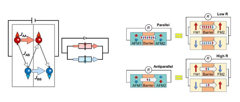
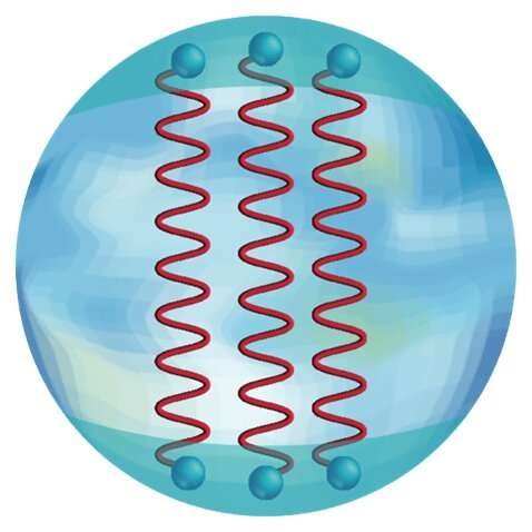
Left: An antiferromagnet can function as “parallel electrical circuits” carrying Néel spin currents. Right: A tunnel junction based on the antiferromagnets hosting Néel spin currents can be regarded as “electrical circuits” with the two ferromagnetic tunnel junctions connected in parallel. Credit: Shao Dingfu
A group of physicists at Hefei Institutes of Physical Science (HFIPS) of Chinese Academy of Sciences (CAS) revealed a secret of antiferromagnets, which could accelerate spintronics, a next-gen data storage and processing technology for overcoming the bottleneck of modern digital electronics.
This finding was reported in Physical Review Letters.
Spintronics is a vigorously developing field employing the spin of electrons within magnetic materials to encode information. Spin-polarized electric currents play a central role in spintronics, due to the capabilities of manipulation and detection of magnetic moment directions for writing and reading 1s and 0s. Currently, most spintronic devices are based on ferromagnets, where the net magnetizations can efficiently spin polarize electric currents.
Antiferromagnets, with opposite magnetic moments aligned alternately, are less investigated but may promise even faster and smaller spintronic devices. However, antiferromagnets have zero net magnetization and thus are commonly believed to carry solely spin-neutral currents useless for spintronics. While antiferromagnets consist of two antiparallel aligned magnetic sublattices, their properties are deemed to be “averaged out” over the sublattices making them spin independent.
Prof. Shao Ding-Fu, who led the team, has a different point of view in this research. He envisioned that collinear antiferromagnets can function as “electrical circuits” with the two magnetic sublattices connected in parallel. With this simple intuitive picture in mind, Prof. Shao and his collaborators theoretically predicted that magnetic sublattices could polarize the electric current locally, thus resulting in the staggered spin currents hidden within the globally spin-neutral current.
He dubbed these staggered spin currents as “Néel spin currents” after Louis Néel, a Nobel laureate, who won the prize due to the fundamental work and discoveries concerning antiferromagnetism.
The Néel spin currents is a unique nature of antiferromagnets which has never been recognized. It is capable to generate useful spin-dependent properties which have been previously considered incompatible with antiferromagnets, such as a spin-transfer torque and tunneling magnetoresistance in antiferromagnetic tunnel junctions, crucial for electrical writing and reading of information in antiferromagnetic spintronics.
“Our work uncovered a previously unexplored potential of antiferromagnets, and offered a straightforward solution to achieve the efficient reading and writing for antiferromagnetic spintronics,” said Prof. Shao Ding-Fu.
More information: Ding-Fu Shao et al, Néel Spin Currents in Antiferromagnets, Physical Review Letters (2023). DOI: 10.1103/PhysRevLett.130.216702

. DOI: 10.1038/s41567-023-02084-6")


. DOI: 10.1080/21663831.2023.2224396")


. All wavenumbers between 800 and 4800 cm−1 (2.1–12 μm) are covered. The pulse width is 2 ps with a bandwidth of 8–10 cm−1 according to the manufacturer (APE Angewandte Physik & Elektronik GmbH, Berlin, Germany). Credit: Nature Photonics (2023). DOI: 10.1038/s41566-023-01243-8")
 and graduate student Dongkwan Lee (right) demonstrate operation of the BonFIRE microscopy apparatus. Credit: Caltech")

. DOI: 10.1038/s41566-023-01217-w")

 placed in front of the coherent fiber bundle. Scanning electron microscope imagesof the meta-optic (right) show the individual scatterer, which spans the entire aperture of the device. Credit: Johannes E. Fröch, Luocheng Huang, Quentin A.A. Tanguy, Shane Colburn, Alan Zhan, Andrea Ravagli, Eric J. Seibel, Karl Böhringer, Arka Majumdar")