Over the past few years, researchers have developed various quantum technologies, alternatives to classical devices that operate by leveraging the principles of quantum mechanics. These technologies have the potential to outperform their classical counterparts in specific settings or scenarios.
Among the many quantum technologies proposed and devised so far are quantum batteries, energy storage devices that could theoretically store energy more efficiently than classical batteries, while also charging more rapidly. Despite their predicted potential, most quantum battery solutions proposed to date have not yet proven to exhibit a genuine quantum advantage, or in other words, to perform better than their classical counterparts.
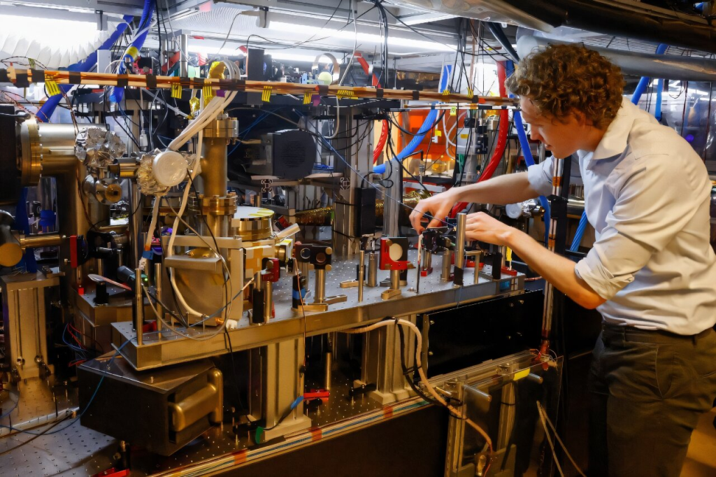
Researchers at PSL Research University and the University of Pisa recently introduced a new deceptively simple quantum battery model that could exhibit a genuine quantum advantage over a classical analog battery. The new model, outlined in a paper published in Physical Review Letters, was found to successfully reach the so-called quantum speed limit, the maximum speed that a quantum system could theoretically achieve.
“Quantum batteries are microscopic devices that can exhibit quantum advantages over their classical counterparts in energy-related tasks,” Vittoria Stanzione and Gian Marcello Andolina, co-authors of the paper, told Phys.org. “This research area originated from quantum information theory, which predicts that quantum resources—such as entanglement—can dramatically enhance the charging power of quantum systems.
“In recent years, some of the authors of the present work proposed a model displaying such a quantum advantage: the Sachdev–Ye–Kitaev (SYK) model. However, this model is highly complex, both experimentally—due to its many-body interactions—and theoretically, as it is analytically challenging.”
Earlier works demonstrating a quantum advantage of batteries based on the SYK model only did so using numerical simulations, without performing any further analyses. Building on their earlier efforts, Stanzione, Andolina and their colleagues tried to identify the simplest possible quantum battery model that could display a quantum advantage in terms of charging power.
“Our model consists of two coupled harmonic oscillators: one acts as the ‘charger,’ and the other serves as the ‘battery,'” explained Stanzione and Andolina. “The key ingredient enabling the quantum advantage is an anharmonic interaction between the two oscillators during the charging process. This anharmonic coupling allows the system to access non-classical, entangled states that effectively create a ‘shortcut’ in Hilbert space, enabling faster energy transfer than in classical dynamics.”
To rigorously certify their model’s quantum advantage, the researchers compared it to a suitable classical battery model, while also implementing a formal bound that was outlined by Maciej Lewenstein and other researchers at the Institute of Photonic Sciences (ICFO) in Barcelona. Overall, their findings suggest that their quantum battery model does outperform its classical counterpart.
“To the best of our knowledge, this work provides the first rigorous certification of a genuine quantum advantage in a solvable model,” said Stanzione and Andolina. “Furthermore, the proposed setup can be realized with current experimental technologies.”
So far, the researchers’ model is merely theoretical, and much work still needs to be done before it can be realized experimentally. In their paper, the team briefly explores the possibility of realizing their proposed battery model using superconducting circuits, which are electrical circuits made of materials that exhibit a resistance of zero at low temperatures.
“We now plan to collaborate with experimental groups in the future to pursue a proof-of-principle realization,” added Stanzione and Andolina. “At the same time, the development of a fully functional quantum battery—integrated with other quantum technologies—remains a distant goal. We hope that our work will stimulate further research on this exciting topic, fostering progress on both the theoretical and experimental fronts.”
For decades, ferromagnetic materials have driven technologies like magnetic hard drives, magnetic random access memories and oscillators. But antiferromagnetic materials, if only they could be harnessed, hold out even greater promise: ultra-fast information transfer and communications at much higher frequencies—a “holy grail” for physicists.
Now, researchers have taken a meaningful step towards utilizing antiferromagnets for new technologies. In “Spin-filter tunneling detection of antiferromagnetic resonance with electrically-tunable damping,” published in Science, they describe their innovative approach for both detecting and controlling the motion of spins within antiferromagnets using 2D antiferromagnetic materials and tunnel junctions.
Both types of materials contain atoms that act like tiny individual magnets, each having “spin.” In a ferromagnet, all of these atomic spins are aligned, producing an external magnetic field. In an antiferromagnet, atomic spins cancel when they are added up, so no external magnetic field is produced. That’s why it’s difficult to not only detect the motions of spins within antiferromagnets but also control the motion of their spins.
Previously, detections of the spin dynamics in antiferromagnets occurred with millimeter or larger samples, “not something that really scales down to any kind of useful device scale,” said co-corresponding author Dan Ralph, F.R. Newman Professor of Physics in the College of Arts and Sciences and a member of the Kavli Institute at Cornell.
“What we’ve done is make micrometer-scale devices where we can see strong signals, using tunnel junctions to be able to detect the spin motions electrically—and that’s nearly a factor of 1,000 smaller than what’s been done before.”
Tunneling is a sort of quantum mechanical leaking of an electron through a barrier that a classical particle wouldn’t be able to get through; it’s not a direct flow of electrons across, but a penetration of an electron wave function as it goes through a barrier, Ralph said.
“Electrons can do funny things,” he said, adding that tunneling is a common device used in all kinds of technologies.
When the spins in the antiferromagnet change their directions inside a tunnel junction, this changes the electrical resistance associated with the tunneling electrons, providing a way to measure the spin dynamics.Simulated antiferromagnatic dynamics from numerical integration of the coupled LLGS equations. Credit: Science (2025). DOI: 10.1126/science.adq8590
This electrical detection works at very high speeds. Most technologies are not equipped to detect at that frequency.
“This is one of our breakthroughs: that we’re using this tunneling behavior, which is this quantum mechanical electron behavior, to really read out these extremely fast oscillations,” said co-corresponding author Kelly Luo, a former Presidential Postdoc/Kavli Institute at Cornell Experimental Fellow at Cornell, now an assistant professor at the University of Southern California.
Their breakthroughs came in part by interweaving two fields: 2D materials and spintronics, also known as spin electronics, said lead author Thow Min Jerald Cham, Ph.D.
To help control the spins within the 2D antiferromagnet, the researchers used a mechanism known as spin-orbit torque. They passed a charge current through a material to make a spin current that can interact with the magnet, to apply a torque to the magnet and make it move.
“We were mainly searching for a way to manipulate the spins so that we could detect the 2D layers separately, and we couldn’t really distinguish which layer was doing what. Then we came up with this idea, where we could break the symmetry by twisting the layers,” said Cham, who is now a postdoctoral scholar at California Institute of Technology.
“With this geometry, we can use applied currents with spin-orbit torque to apply a force to just one of the spin layers and not the other, a first step for controlling the spin dynamics,” Ralph said.
“Our studies show that antiferromagnetic materials have great potential,” the researchers wrote, “for realizing nano-oscillators for high-frequency applications.” This is an avenue they continue to explore.
Other co-authors are Xiaoxi Huang, postdoctoral associate in Ralph’s lab; Daniel G. Chica and Xavier Roy, Columbia University; and Kenji Watanabe and Takashi Taniguchi, National Institute for Materials Science, Japan.
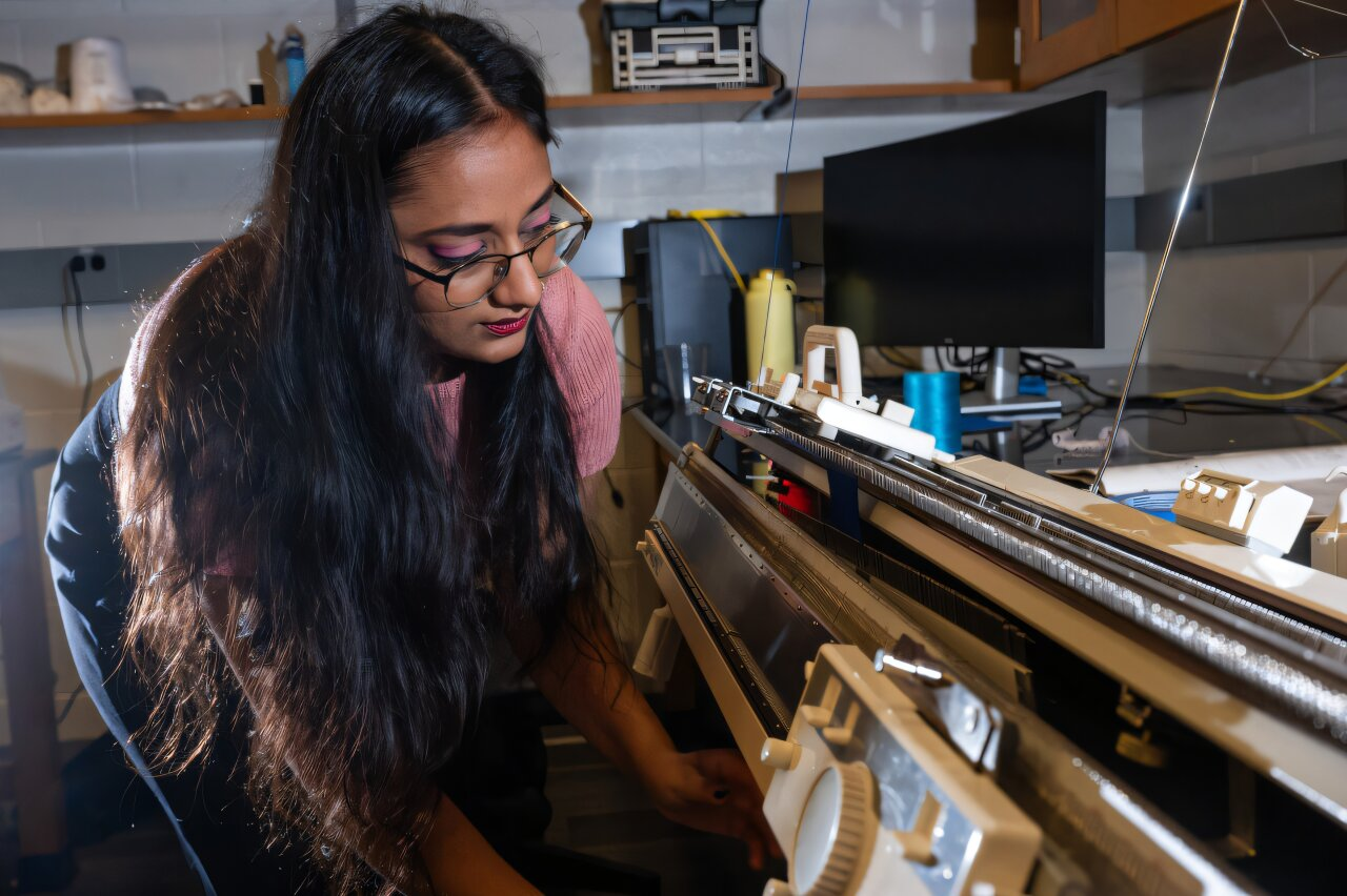
School of Physics Associate Professor Elisabetta Matsumoto is unearthing the secrets of the centuries-old practice of knitting through experiments, models, and simulations. Her goal? Leveraging knitting for breakthroughs in advanced manufacturing—including more sustainable textiles, wearable electronics, and soft robotics.
Matsumoto, who is also a principal investigator at the International Institute for Sustainability with Knotted Chiral Meta Matter (WPI-SKCM2) at Hiroshima University, is the corresponding author on a new study exploring the physics of ‘jamming’—a phenomenon when soft or stretchy materials become rigid under low stress but soften under higher tension.
The study, “Pulling Apart the Mechanisms That Lead to Jammed Knitted Fabrics,” is published in Physical Review E, and also includes Georgia Tech Matsumoto Group graduate students Sarah Gonzalez and Alexander Cachine in addition to former postdoctoral fellow Michael Dimitriyev, who is now an assistant professor at Texas A&M University.
The work builds on the group’s previous research demonstrating that knitted materials can be mathematically “programmed” to behave in predictable ways. “These properties are intuitively understood by people who knit by hand,” Matsumoto says, “but in order to manipulate and use these behaviors in an industrial setting, we need to understand the physics behind them. This new research is another step in that direction.”
An unexpected twist Gonzalez, who led the research, first became interested in jamming while conducting adjacent research. “I was using model simulations to characterize how different yarn properties affect the behavior of knitted fabrics and noticed a strange stiff region,” she recalls. “In our previous research, we had also seen this behavior in lab experiments, which suggested that what we were seeing in the simulations was a genuine phenomenon. I wanted to investigate it further.”
After digging into the topic, she realized that what she was seeing was called ‘jamming.” In knits, Gonzalez explains, jamming occurs when stitches are packed tightly together, and the fabric resists stretching. Although it’s a well-known phenomenon, the physics has mostly been investigated in granular systems, like snow or sand, rather than fabrics.
“In fabrics, when you pull softly, the response is surprisingly stiff, but when you start pulling harder and harder, the stitches rearrange, and the material softens,” Matsumoto says. “In granular systems, this is a little like how avalanches work. At low forces, the snow pack is solid, but when the slope is steep, the force of gravity liquidizes that snow pack into an avalanche.”
“In fabrics, it is a little like having a tangle in a piece of jewelry,” she adds. “If you pull on it, it gets quite stiff, but if you loosen the knot, the chain can reconfigure, and it’s not so stiff.”
Unraveling the physics of jamming
Using a combination of experiments with industrially knitted fabrics and computer models, the team analyzed what causes jamming in fabrics and how to control it. “We wanted to determine how different yarn properties impacted jamming,” Gonzalez explains. “Our goal was to understand the mechanics of jamming through how yarn interacts at various touchpoints in stitches.”
The team found that both machine tension and yarn thickness played a key role in making a fabric more or less jammed, and that jamming behaves differently depending on which direction the fabric is stretched.
“When you stretch a knit along the rows, the stiffness of the yarn causes fabric jamming. Jamming in the other direction is due to yarn contacts,” says Gonzalez. “We also showed that the impacts of changing machine tension and yarn thickness differ depending on fabric direction.”
“Discovering that fabric jamming works differently in different directions was a key insight,” she adds. “To our knowledge, the physics of this has never been explored before.”
Modern innovation—with a centuries-old technique
The research dovetails with Matsumoto’s WPI-SKCM2 Center work, which involves investigating fundamental aspects of knots and chirality. The Center is interested in a class of materials called “knotted chiral meta matter” that could lead to more sustainable materials.
For example, knitting—which leverages chiral knots—could be used to create more elastic fabrics from natural materials. “In many cases, manufacturers use yarns that combine, for example, polyester, cotton, and elastane to create a desired elasticity,” Matsumoto says. “Our research suggests that manipulating the topology of the stitches could lead to a similar elasticity, reducing the need for petroleum-based fibers and creating a more sustainable textile.”
“Knitting has the potential to be extremely useful in manufacturing, but knowledge has typically been shared through intuition and word of mouth,” she adds. “By creating these mathematical models, we hope to formalize that knowledge in a way that’s accessible for large-scale manufacturing—so we can leverage this centuries-old intuition for modern innovation.”
It is now understood that all known matter, i.e., studied by science and harnessed by technology, constitutes only 5% of the content of the universe. The rest is composed of two unknown components: dark matter (about 27%) and dark energy (about 68%). This calculation, confirmed decades ago, continues to surprise both lay people and scientists alike.
In the case of dark matter (DM), there is abundant evidence that it really exists, all resulting from its gravitational interaction with ordinary matter. This evidence comes from sources such as the rotation curves of stars in galaxies, discrepancies in the movement of galaxies in clusters, the formation of large-scale structures in the universe, and cosmic background radiation, which is distributed uniformly throughout space.
Despite knowing with a high degree of certainty that DM exists, we do not know what it is. Several models proposed thus far have failed.
A new study by researchers at the University of São Paulo (USP) in Brazil proposes an inelastic DM model that interacts with ordinary matter through a vector mediator similar to a photon, but with mass. The aim is to open a new window of observation. An article on the subject is published in the Journal of High Energy Physics.
“In this work, we consider a DM model composed of a dark sector with light particles that interact weakly with the known particles of the Standard Model [SM],” says Ana Luisa Foguel, a Ph.D. student at the Physics Institute (IF-USP) and the first author of the article.
Initially, the search for DM focused on heavy candidates with masses much greater than that of an electron or even the heaviest particles in the SM. The idea was that, because they were so massive, these particles could not be produced by particle colliders, which did not yet have sufficient energy. However, even with the experiments carried out at the Large Hadron Collider (LHC) at the European Organization for Nuclear Research (CERN, in its official French acronym), no new particles beyond those of the SM have been observed.
Consequently, some in the scientific community shifted their focus to searching for light particles with extremely weak interactions. The idea was that such particles had not yet been observed because they interact very weakly with ordinary matter. To investigate signs of these particles, experiments needed to move toward the so-called “intensity frontier,” meaning they would have to measure couplings and interactions with increasing precision to detect any discrepancies that might signal the existence of something new.
Thermal freeze-out
The study is moving in this direction.
“When considering a new DM model, the first thing is to know how it was possible to produce the right amount of such a component. This amount is now measured very precisely, with data from cosmic background radiation, for example. And several mechanisms are known that could have led to the generation of DM in the early universe. One of the most theoretically motivated is the so-called ‘thermal freeze-out,'” says Foguel.
In particle physics and cosmology, thermal freeze-out is the moment when certain particles decouple from the thermal bath, meaning the interactions that transform these particles into other SM particles are no longer sufficient. After this point, since there are no processes that can alter the number of these particles, their abundance “freezes,” remaining virtually unchanged.
“This mechanism is interesting and well known, as we have several examples of SM particles whose abundance was generated in this way. Therefore, it’s natural to consider that the components of DM were generated by a similar mechanism,” comments the researcher.
In this mechanism, DM candidate particles are in a “thermal bath” with ordinary matter particles shortly after the beginning of the universe. In other words, all particles interact very quickly to share the same temperature. As the universe expands and cools, the particles lose this thermal contact. This process is called “freeze-out.”
“The exact moment of decoupling depends on the probability of interactions between DM particles and SM particles. This probability is parameterized by a variable we call the sigma shock section. If sigma is very small, DM particles decouple very early and their abundance is very high. Conversely, if it’s very large, the DM remains in thermal contact longer, annihilating itself into SM particles, so that when it decouples later, it doesn’t have sufficient abundance,” points out Foguel.
In the case of light DM, the interaction with ordinary matter occurs through a portal. In other words, DM particles do not couple directly with all SM particles, but rather with a mediator particle that facilitates interaction between DM and the SM. The sigma shock section of this interaction is proportional to the mass of the DM and inversely proportional to the mass of the portal particle.
Thus, for a light candidate to exist at an energy level below gigaelectronvolts, the portal cannot be too heavy. Therefore, the SM bosons that mediate weak interactions (W+, W-, and Z0) would not function as portals. A new dark particle must be introduced to mediate between the DM and the SM.
“In our model, this particle that mediates the relationship between the two sectors is a vector boson (ZQ). It behaves like a photon, the particle that mediates electromagnetic interactions, but it has mass. In addition, the difference in this model is that this mediator also interacts directly with other SM particles,” says the researcher.
This mediator would connect the SM particles to the DM particles. According to the proposed model, there are two types of these particles: a stable particle (χ₁), which would make up DM itself, and a slightly heavier unstable particle (χ₂). These particles would always interact with the ZQ mediator together. In other words, the mediator would interact with both at the same time. This would constitute a specific type of DM called “inelastic dark matter.”
In addition, χ₂ could decay into χ₁ and SM particles. This work demonstrates that these arrangements can explain the abundance of DM in the universe while circumventing the experimental limits that prevent its detection.
“It’s worth noting that models such as ours, with inelastic DM, are interesting because in addition to explaining the efficient generation of DM through the freeze-out mechanism, they also make it possible to circumvent the current limits of direct and indirect detection, as well as the limits of cosmology. The reason comes from the fact that as χ₂ isn’t stable and interactions depend on χ₂, there isn’t enough χ₂ population during the recombination epoch to inject energy into the plasma, which could have modified the cosmic background radiation.
“And there’s also no χ₂ in the current universe to decay or annihilate with χ₁, producing signals that enable indirect detection. Furthermore, for χ₁ to interact in direct detection experiments, it’d have to transform into χ₂, which is very difficult because χ₂ is more massive,” Foguel explains.
Overcoming the ‘vanilla’ model According to the researcher, the proposed new model would serve as an alternative to the “vanilla” model of inelastic DM, which considers a mediator that does not couple directly with DM particles. In particle physics, “vanilla” is used to designate the most basic and minimalist version of a model with the fewest theoretical ingredients possible.
“The vanilla model has already been practically ruled out, because almost all of the parameters that reproduce the correct abundance of DM have been discarded by experimental searches. Thus, the main objective of our work was to show that by considering a simple modification of this model—allowing mediators with direct rather than indirect couplings—we can potentially ‘save’ inelastic DM,” Foguel explains.
“Considering the proposed models, we first calculated the abundance of DM using the freeze-out process and made a code available online that allows these calculations to be reproduced, showing the regions of the parameter space that produce inelastic DM for different choices of Q load, with correct abundance. After that, we focused on the limits of different experiments.
“We concluded that for certain models, new regions of the parameter space are ‘unlocked,’ that is, there are parameters that reproduce the correct abundance of DM and haven’t yet been excluded. Some of these parameter regions could be investigated in future experiments.”
Renata Zukanovich Funchal, a full professor at IF-USP, Foguel’s advisor, study coordinator, and co-author of the article, summarizes, “The use of more general vector mediators opens a new window for viable models of inelastic DM, with direct consequences for decay rates, experimental signatures, and cosmological limits.”
Scientists at the Institute for Photonic Quantum Systems (PhoQS) and the Paderborn Center for Parallel Computing (PC2) at Paderborn University have developed a powerful open-source software tool that allows them to simulate light behavior in quantum systems.
The unique feature of this tool, named “Phoenix,” is that researchers can use it to very quickly investigate complex effects to a level of detail that was previously unknown, and all without needing knowledge of high-performance computing. The results have now been published in Computer Physics Communications.
Phoenix solves equations that describe how light interacts with material at the quantum level, which is essential for understanding and for the design of future technologies such as quantum computers and advanced photonic devices.
“More specifically, we are looking here at so-called non-linear Schrödinger and Gross-Pitaevskii equations in two spatial dimensions. Phoenix’s design means that it can run on standard laptops or high-performance GPUs and is up to a thousand times faster and up to 99.8% more energy-efficient than conventional tools,” explains Professor Stefan Schumacher from PhoQS.
Phoenix is available to researchers anywhere in the world free of charge. The software is already being used to study new physical effects in rare quantum states of light and has the ability to help scientists to better understand and monitor light at the smallest scales.
Ph.D. student Jan Wingenbach, who is the lead author of the current study, adds, “Optimization to the current level was only possible through our close cooperation with the HPC [high Performance Computing] experts from PC2.”
“This synergy between cutting-edge research in quantum photonics and high-performance computing has made it possible for us to extend the limits of computing power and capability,” adds Dr. Robert Schade, research assistant and HPC expert at PC2.
Preliminary versions of the Phoenix code have already contributed to important breakthroughs in quantum photonics. According to the team, the program will be an important computational tool for research into new photonic states and their interactions.
Quantum computers, devices that can perform computations relying on the principles of quantum mechanics, are expected to outperform classical computers on some types of optimization and processing tasks. While physicists and engineers have introduced various quantum computing systems over the past decades, reliably scaling these systems so that they can tackle real-world problems while correcting errors arising during computations has so far proved challenging.
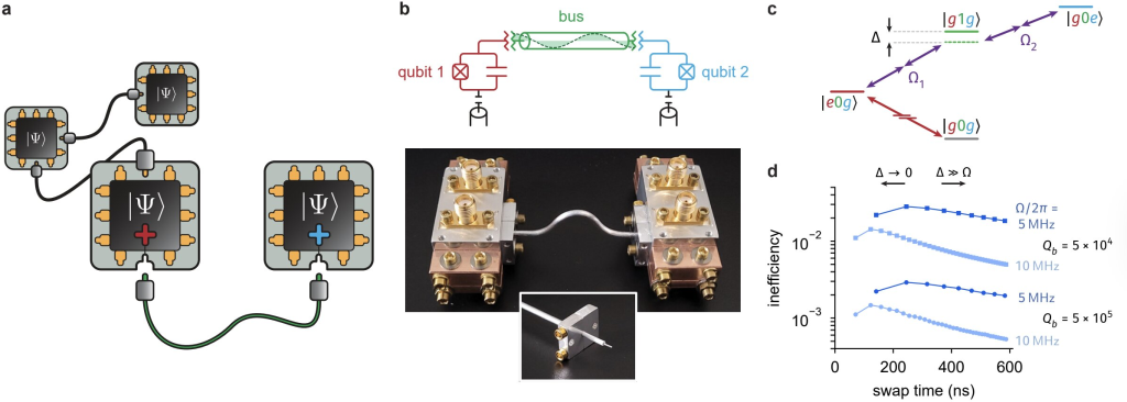
Researchers at the University of Illinois at Urbana-Champaign recently introduced a new, modular quantum architecture for scaling superconducting quantum processors in a fault-tolerant, scalable and reconfigurable way. Scaling in a fault-tolerant way is required to maintain the quantum effects and conditions necessary to perform long-term quantum computations.
Their proposed system, outlined in a paper published in Nature Electronics, is comprised of several modules (i.e., superconducting qubit devices) that can operate independently and be connected to others via a low-loss interconnect, forming a larger quantum network.
“The starting point for this study was current insight in the field of superconducting quantum computing that we will need to break out processors into multiple independent devices—an approach we call ‘modular quantum computing,'” Wolfgang Pfaff, senior author of the paper, told Phys.org.
“This has, in the last years, become a widespread belief, and even companies like IBM are pursuing it. We wanted to know if we can realize an engineering-friendly interconnect for this approach.”
Essentially, Pfaff and his colleagues wanted to devise a strategy to connect quantum devices while minimizing signal degradation or energy dissipation when quantum information is transmitted between them. Moreover, they wanted to be able to easily connect, disconnect and reconfigure the devices.
“Very simply speaking, our approach entails the use of a high-quality superconducting coaxial cable called a bus-resonator,” explained Pfaff. “We connect a qubit capacitively to a cable through a custom connector that places the cable very close (sub-mm precision) to the qubit. This allows us then to effectively perform gates between qubit and cable, and then multiple qubits if they are connected to the same cable.
“The key in what we’ve shown is the ability to combine a very low-loss connection between the cable and the qubit with a fast and high-efficiency gate; that gate is also a new development by us, by exploiting a fast frequency-conversion process that our style of qubits (transom qubits) allows us to do.”
The researchers’ new approach for creating modular quantum networks has notable advantages over previous methods to scale quantum systems. In initial tests, they found that it allowed them to robustly connect superconductor-based quantum devices and disconnect them later without damaging them; all without introducing significant signal loss in quantum gates.
“Using our approach, I think that we have opportunities to build reconfigurable quantum systems from the bottom up, with, for example, the option to over time ‘plug in’ more processor modules to a network of quantum devices,” added Pfaff.
“We are currently working on a design in which we want to see if we can increase the number of elements that we are connecting, making our networks larger. We are also exploring how we can better overcome losses in the system and make the architecture compatible with quantum error correction.”
The theory of quantum mechanics has transformed daily life since being proposed a century ago, yet how it works remains a mystery—and physicists are deeply divided about what is actually going on, a survey in the journal Nature said Wednesday.
“Shut up and calculate!” is a famous quote in quantum physics that illustrates the frustration of scientists struggling to unravel one of the world’s great paradoxes.
For the last century, equations based on quantum mechanics have consistently and accurately described the behavior of extremely small objects.
However, no one knows what is happening in the physical reality behind the mathematics.
The problem started at the turn of the 20th century, when scientists realized that the classical principles of physics did not apply to things on the level of atoms.
Bafflingly, photons and electrons appear to behave like both particles and waves. They can also be in different positions simultaneously—and have different speeds or levels of energy.
In 1925, Austrian physicist Erwin Schroedinger and Germany’s Werner Heisenberg developed a set of complex mathematical tools that describe quantum mechanics using probabilities.
This “wave function” made it possible to predict the results of measurements of a particle.
These equations led to the development of a huge amount of modern technology, including lasers, LED lights, MRI scanners and the transistors used in computers and phones.
But the question remained: what exactly is happening in the world beyond the math?
A confusing cat To mark the 100th year of quantum mechanics, many of the world’s leading physicists gathered last month on the German island of Heligoland, where Heisenberg wrote his famous equation.
More than 1,100 of them responded to a survey conducted by the leading scientific journal Nature.
The results showed there is a “striking lack of consensus among physicists about what quantum theory says about reality,” Nature said in a statement.
More than a third—36%—of the respondents favored the mostly widely accepted theory, known as the Copenhagen interpretation.
In the classical world, everything has defined properties—such as position or speed—whether we observe them or not.
But this is not the case in the quantum realm, according to the Copenhagen interpretation developed by Heisenberg and Danish physicist Niels Bohr in the 1920s.
It is only when an observer measures a quantum object that it settles on a specific state from the possible options, goes the theory. This is described as its wave function “collapsing” into a single possibility.
The most famous depiction of this idea is Schroedinger’s cat, which remains simultaneously alive and dead in a box—until someone peeks inside.
The Copenhagen interpretation “is the simplest we have,” Brazilian physics philosopher Decio Krause told Nature after responding to the survey.
Despite the theory’s problems—such as not explaining why measurement has this effect—the alternatives “present other problems which, to me, are worse,” he said.
Enter the multiverse But the majority of the physicists supported other ideas.
Fifteen percent of the respondents opted for the “many worlds” interpretation, one of several theories in physics that propose we live in a multiverse.
It asserts that the wave function does not collapse, but instead branches off into as many universes as there are possible outcomes.
So when an observer measures a particle, they get the position for their world—but it is in all other possible positions across many parallel universes.
“It requires a dramatic readjustment of our intuitions about the world, but to me that’s just what we should expect from a fundamental theory of reality,” US theoretical physicist Sean Carroll said in the survey.
The quantum experts were split on other big questions facing the field.
Is there some kind of boundary between the quantum and classical worlds, where the laws of physics suddenly change?
Forty-five percent of the physicists responded yes to this question—and the exact same percentage responded no.
Just 24% said they were confident the quantum interpretation they chose was correct.
And three quarters believed that it will be replaced by a more comprehensive theory one day.
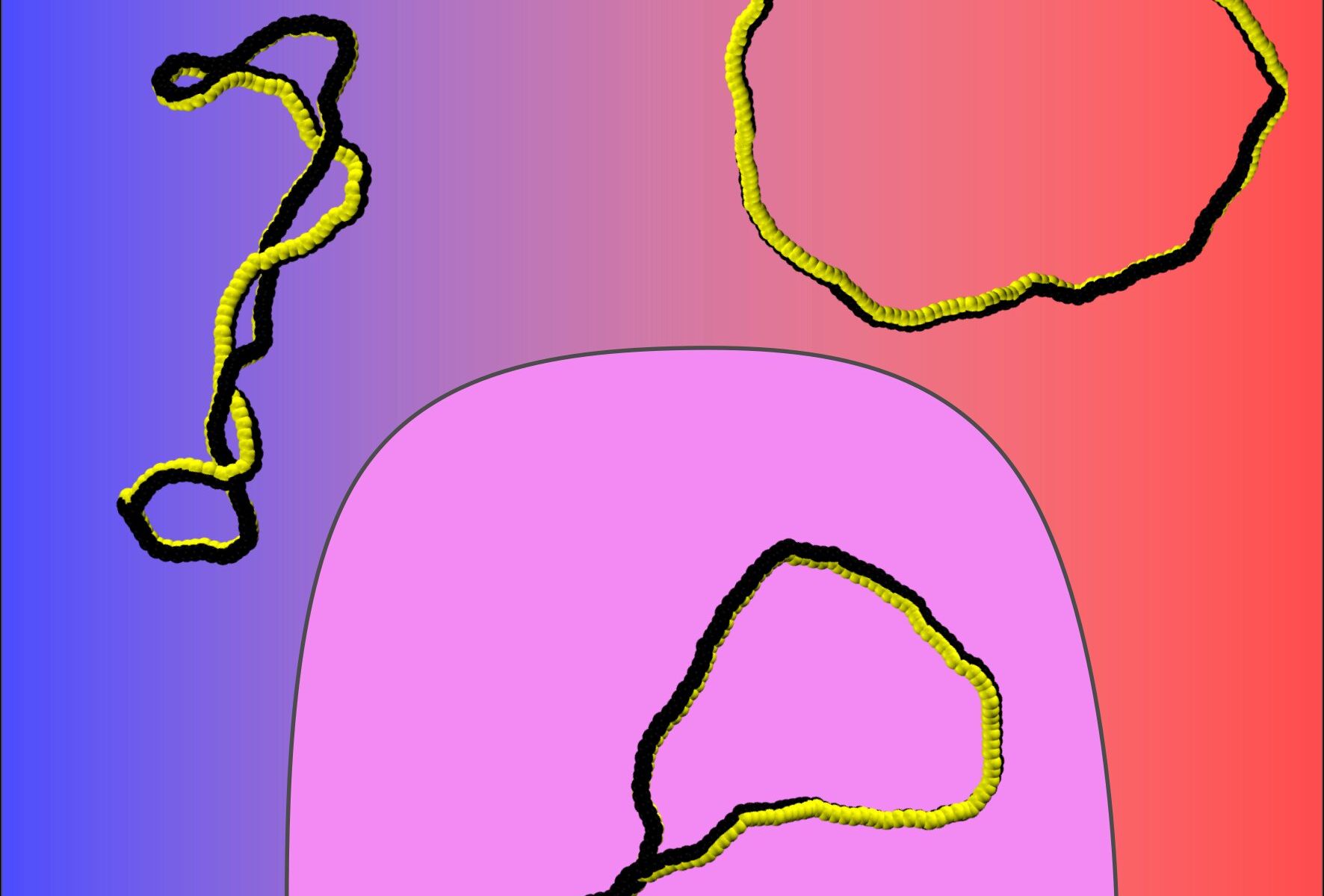
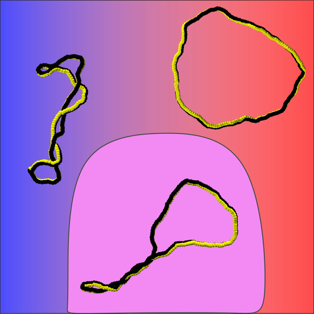
What if a complex material could reshape itself in response to a simple chemical signal? A team of physicists from the University of Vienna and the University of Edinburgh has shown that even small changes in pH value and thus in electric charge can shift the spatial arrangement of closed ring-shaped polymers (molecular chains)—by altering the balance between twist and writhe, two distinct modes of spatial deformation.
Their findings, published in Physical Review Letters, demonstrate how electric charge can be used to reshape polymers in a reversible and controllable way—opening up new possibilities for programmable, responsive materials.
With such materials, permeability and mechanical properties such as elasticity, yield stress and viscosity could be better controlled and precisely “programmed.”
Imagine taking a ribbon and twisting it in half before connecting its ends: you create the famous Möbius band—a loop with a single twist and a continuous surface. Add more twists before closing the ribbon, and the structure becomes so-called supercoiled.
Such shapes are common in biology and materials science, especially in circular DNA and synthetic (artificially produced) ring polymers. Whether and how the balance between twisty—the local rotation of the ribbon around its axis—and writhe—the large-scale coiling of the ribbon in space, could be tuned in a controlled and reversible way, is still unclear.
The research team set out to investigate this question using a model system of ring-shaped polymers, where electric charge—introduced via pH-dependent ionization—serves as an external tuning parameter.
From writhe to twist To explore the tunability of this topological balance, the researchers combined computer simulations and analytical theory to study how charge affects the conformation of supercoiled ring polymers.
In their model, each monomeric unit acts as a weak acid, gaining or losing charge depending on the pH value (specifies the acidity or basicity of aqueous solutions) of the surrounding solution. This setup enabled a gradual buildup of charge and revealed how the molecule reshapes in response.
The results: Neutral polymers adopt writhe-rich, compact shapes. As charge increases, electrostatic repulsion grows—driving the molecule toward more extended conformations and shifting the internal distribution from writhe to twist. These transitions are smooth at low supercoiling.
At higher levels, however, the model predicts a striking feature: the polymer can split into coexisting twist- and writhe-rich domains—a kind of topologically constrained microphase separation. This hidden form of phase coexistence had not been observed in such systems before.
To capture these mechanisms, the researchers developed a Landau-type mean-field theory. This simplified mathematical model accurately predicts when a polymer will undergo a continuous or abrupt conformational change—depending on its degree of supercoiling and charge.
Topology as a design tool
The idea of tuning not just molecular structure, but topology itself, opens up new ways to control responsive systems. “By adjusting the local charge, we can shift the balance between twist and writhe—and that gives us a handle on the shape of the whole molecule,” says first author Roman Staňo from the Faculty of Physics at the University of Vienna (currently at Cambridge University).
Because each monomer can gain or lose charge, the polymer gradually reshapes itself—a behavior that resembles real polyelectrolytes, such as chemically modified DNA.
The team suggests that synthetic DNA rings with pH-sensitive side chains—not yet realized experimentally, but now feasible thanks to recent advances in nucleotide chemistry—could display this kind of controllable shape-shifting behavior. These molecules would act as topologically constrained scaffolds, adjusting their form in response to local chemical conditions.
Responsive shapes, programmable function
Polymer shape isn’t just geometry—it governs flow, function, and interaction. The ability to reversibly shift between twist- and writhe-dominated states offers a powerful strategy for designing adaptive materials. Ring polymers that respond to subtle changes in pH could one day be used in microfluidic devices, where local conditions trigger controlled changes in shape and flow behavior.
“What’s remarkable,” says co-author Christos Likos, Faculty of Physics at the University of Vienna, “is that the transition from compact to extended shapes happens gradually, can be controlled via pH and doesn’t require any changes to the molecule’s topology.”
This effect, the team notes, could be realized experimentally in synthetic DNA rings—a possibility enabled by recent advances in nucleotide chemistry.
Their results also offer predictive insight: they show how function can be encoded not only in chemical composition, but also in a topological state—pointing toward a new generation of shape-adaptive materials.
Engineers at the UCLA Samueli School of Engineering have introduced a universal framework for point spread function (PSF) engineering, enabling the synthesis of arbitrary, spatially varying 3D PSFs using diffractive optical processors. The research is published in the journal Light: Science & Applications.
This framework allows for advanced imaging capabilities—such as snapshot 3D multispectral imaging—without the need for spectral filters, axial scanning, or digital reconstruction.
PSF engineering plays a significant role in modern microscopy, spectroscopy and computational imaging. Conventional techniques typically employ phase masks at the pupil plane, which constrain the complexity and mathematical representation of the achievable PSF structures.
The approach developed at UCLA enables arbitrary, spatially varying 3D PSF engineering through a series of passive surfaces optimized using deep learning algorithms, forming a physical diffractive optical processor.
Through extensive analyses, the researchers showed that these diffractive processors can approximate any linear transformation between 3D optical intensity distributions in the input and output volumes. This enables precise, diffraction-limited control of light in three dimensions, paving the way for highly customized and sophisticated optical functions for 3D optical information processing.
By jointly engineering the spatial and spectral properties of 3D PSFs, the framework supports powerful imaging modalities such as snapshot 3D multispectral imaging—achieved without mechanical scanning, spectral filters, or computational postprocessing. This all-optical approach offers unmatched versatility for high-speed, high-throughput optical systems.
This work marks a significant stepping-stone for future advances in computational imaging, optical sensing and spectroscopy, as well as 3D optical information processing. Potential applications include compact multispectral imagers, high-throughput 3D microscopy platforms, and novel optical data encoding and transmission systems.
The study was conducted by Dr. Md Sadman Sakib Rahman and Dr. Aydogan Ozcan in the UCLA Electrical and Computer Engineering Department and the California NanoSystems Institute (CNSI).
Researchers developed a single-photon Raman lidar system that operates underwater and can remotely distinguish various substances They demonstrated the system by using it to detect varying thicknesses of gasoline oil in a quartz cell that was 12 meters away from the system in a large pool. Credit: Mingjia Shangguan, Xiamen University
Researchers report a new single-photon Raman lidar system that operates underwater and can remotely distinguish various substances. They also show that the new system can detect the thickness of the oil underwater up to 12 m away, which could be useful for detecting oil spills.
“Differentiating substances in water and detecting their distribution characteristics in the ocean are of great significance for marine monitoring and scientific research,” said research team leader Mingjia Shangguan from Xiamen University in China. “For instance, the remote sensing of underwater oil that we demonstrated could be useful for monitoring leaks in underwater oil pipelines.”
Although lidar approaches based on Raman signals have been previously used for detection of underwater substances, existing systems are impractical because they are bulky and require large amounts of power.
In the journal Applied Optics, the researchers describe their new lidar system, which uses just 1 μJ of pulse energy and 22.4 mm of receiver aperture. The entire lidar system is 40 cm long with a diameter of 20 cm and can be operated up to 1 km underwater. To boost sensitivity, the researchers incorporated single-photon detection into their compact underwater Raman lidar system.
“Mounting an underwater Raman lidar system on an autonomous underwater vehicle or remotely operated vehicle could enable monitoring for leaks in underwater oil pipelines,” said Shangguan. “It could potentially also be used to explore oceanic resources or be applied in detecting seafloor sediment types, such as coral reefs.”
Single-photon sensitivity in underwater lidar
Traditional lidar systems designed to operate above water on ships, aircraft or satellites can achieve large-scale ocean profiling, but their detection depth is limited, especially during rough sea conditions. Raman lidar systems, however, can be used for analysis underwater at different depths without being affected by sea conditions.
Raman lidar works by emitting a pulse of green laser light into the water that interacts with substances such as oil. This excites inelastic Raman signals that can be used to identify substances. By measuring the intensity of Raman signals at specific wavelengths, lidar can provide information about the oil content in the water.
“Traditional Raman lidar systems rely on increasing laser power and telescope aperture to achieve remote sensing detection, which leads to a large system size and high-power consumption that make it difficult to integrate lidar systems onto underwater vehicles,” said Shangguan. “The use of single-photon detection technology made this work possible by improving detection sensitivity to the level of single photons.”
The researchers demonstrated their new lidar system by using it to detect varying thicknesses of gasoline oil in a quartz cell that was 12 m away from the system. Both the lidar system and the quartz cell were submerged at a depth of 0.6 m underwater in a large pool. The lidar system was able to detect and distinguish all thicknesses of gasoline, which ranged from 1 mm to 15 mm.
The researchers are now working to increase the number of detection channels and the Raman spectral resolution of the single-photon lidar system to enhance its ability to distinguish different substances in water. This would allow it to be used to analyze underwater bubble types and to detect corals and manganese nodules.
More information: Mingjia Shangguan et al, Remote sensing oil in water with an all-fiber underwater single-photon Raman lidar, Applied Optics (2023). DOI: 10.1364/AO.488872