When material goes quantum, electrons slow down and form a crystal

When material goes quantum, electrons slow down and form a crystal
Schematic of the moiré superlattice formed between tungsten diselenide and tungsten disulfide, filled with one charge carrier per moiré unit cell. Credit: Lawrence Berkeley National Laboratory

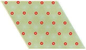
The shifting, scintillating pattern you can see when you stack two slightly misaligned window screens is called moiré. A similar interference effect occurs when scientists stack two-dimensional crystals with mismatched atomic spacings. Moiré superlattices display exotic physical properties that are absent in the layers that make up the patterns. These properties are rooted in the quantum nature of electrons.

Researchers have discovered a new property in the moiré superlattices formed in crystals made of tungsten diselenide/tungsten disulfide(WSe2/WS2). In these two-dimensional crystals, the interactions between electrons become so strong that electrons “freeze” and form an ordered array.

WSe2/WS2 moiré superlattices turn out to be an optimal playground for tuning the interactions between electrons. The stronger these interactions, the more prominent the quantum mechanical nature of solid materials. This allows exotic states of matter like unconventional superconductivity to form.

Researchers used lasers to “observe” the electron motion without the artifacts that plague other measurement techniques. They uncovered a rare quantum state of matter, never before observed in moiré superlattices. Understanding and controlling the quantum motion of electrons will allow scientists to build microelectronic devices of the future and robust qubits for quantum computing.

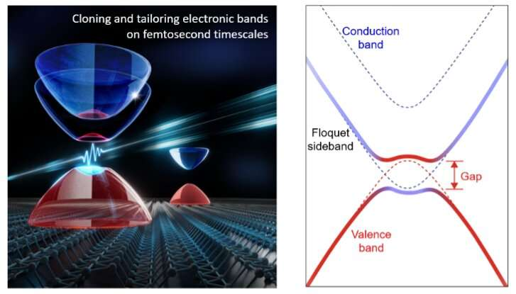
In solids, the energy levels that electrons occupy form energy bands. Moiré superlattices alter the atomic periodicity seen by the electrons and thus the energy bands. Moiré effects can lead to “flat” bands, in which the energy levels are squeezed together, causing electrons to lower their kinetic energy and thus to feel their mutual repulsion more strongly.

A team of researchers at Lawrence Berkeley National Laboratory (LBNL) used a novel optical technique to observe electron motion, while changing the number of electrons injected in the sample. When only one carrier per moiré unit cell was injected, the electrons were expected to move freely and thus conduct electricity. Instead, the sample became insulating. This result illustrates the Mott insulator state, in which electrons interact so strongly that they avoid being in the same cell. If every cell is occupied, then the electrons stop moving.

The real surprise came when fewer electrons were injected so that only one half or one third of the cells were occupied. At these low densities, scientists expected the electrons to feel their presence less and have high mobility. However, the sample turned out an insulator. In WSe2/WS2, electrons interact so strongly that they even avoid sitting on neighboring sites. This rare phenomenon is known as Wigner electron crystal.

LBNL researchers also demonstrated that in WSe2/WS2, light with appropriate polarization interacts with spin-up and spin-down electrons separately, making it possible to selectively change the energy of electrons based on their spin. In doing so, they observed spin excitations persisting orders of magnitude longer than charge excitations. This opens the door for the future investigation of exotic spin states such as quantum spin liquidity.

Related research was previously published in 2020 in the journal Nature.

More information: Emma C. Regan et al, Mott and generalized Wigner crystal states in WSe2/WS2 moiré superlattices, Nature (2020). DOI: 10.1038/s41586-020-2092-4

Journal information: Nature 

Provided by US Department of Energy 
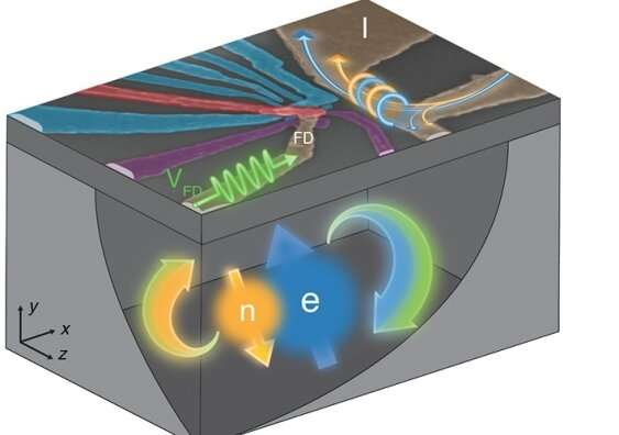
A new neutrino laboratory at the bottom of the Mediterranean for probing sea and sky

A new laboratory at the bottom of the Mediterranean for probing sea and sky
LSPM connection. Credit: Damien Dornic, CPPM, CNRS / PHOTOTHEQUE IN2P3

The Laboratoire Sous-marin Provence Méditerranée (LSPM) lies 40 km off the coast of Toulon, at a depth of 2,450 m, inaccessible even to sunlight. Through this national research platform run by the CNRS in collaboration with Aix-Marseille University (AMU) and IFREMER, scientists will investigate undersea unknowns while scanning the skies for neutrinos. These elementary particles of extraterrestrial origin know few obstacles and can even traverse our planet without bumping into a single atom.

The main instrument at the LSPM is KM3NeT, a giant neutrino detector developed by a team of 250 researchers from 17 countries. In the pitch-black abyss, KM3NeT will study the trails of bluish light that neutrinos leave in the water. Capable of detecting dozens of these particles a day, it will help elucidate their quantum properties, which still defy our understanding.

The other LSPM instruments will permit the scientific community to study the life and chemistry of these depths. They will offer researchers insights into ocean acidification, deep-sea deoxygenation, marine radioactivity, and seismicity, and allow them to track cetacean populations as well as observe bioluminescent animals. This oceanographic instrumentation is integrated into the subsea observatory network of the EMSO European research infrastructure.

LSPM is structured around a series of titanium junction boxes and intelligent systems able to power multiple scientific instruments and retrieve their data in real time, through a 42-km-long electro-optical cable. The base currently has three junction boxes, but the future addition of a second cable could bring the number up to five.

Provided by CNRS 

Unusual atom helps in search for universe’s building blocks

Unusual atom helps in search for Universe's building blocks
Caesium. Credit: The University of Queensland

An unusual form of cesium atom is helping a University of Queensland-led research team unmask unknown particles that make up the universe.

Dr. Jacinda Ginges, from UQ’s School of Mathematics and Physics, said the unusual atom—made up of an ordinary cesium atom and an elementary particle called a muon—may prove essential in better understanding the universe’s fundamental building blocks.

“Our universe is still such a mystery to us,” Dr. Ginges said.

“Astrophysical and cosmological observations have shown that the matter we know about—commonly referred to as ‘Standard Model’ particles in physics—makes up only five percent of the matter and energy content of the universe.”

“Most matter is ‘dark’, and we currently know of no particle or interaction within the Standard Model that explains it.”

“The search for dark matter particles lies at the forefront of particle physics research, and our work with cesium might prove essential in solving this mystery.”

The work may also one day improve technology.

“Atomic physics plays a major role in technologies we use every day, such as navigation with the Global Positioning System (GPS), and atomic theory will continue to be important in the advancement of new quantum technologies based on atoms,” Dr. Ginges said.

Through theoretical research, Dr. Ginges and her team have improved the understanding of the magnetic structure of cesium’s nucleus, its effects in atomic cesium and the effects of the weird and wonderful muon.

“A muon is basically a heavy electron—200 times more massive—and it orbits the nucleus 200 times closer than the electrons,” Dr. Ginges said.

“Because of this, it can pick up on details of the structure of the nucleus.”

“It sounds complicated, but in a nutshell, this work will help to improve atomic theory calculations that are used in the search for new particles.”

The researchers said the new approach can offer greater sensitivity and an alternative technique to finding new particles, through the use of precision atomic measurements.

“You may have heard of the Large Hadron Collider at CERN, the world’s largest and most powerful particle accelerator, which smashes together subatomic matter at high energies to find previously unseen particles,” Dr. Ginges said.

“But our research can offer greater sensitivity, with an alternative technique to find new particles—through precision atomic measurements.”

“It doesn’t need a giant collider, and instead uses precision instruments to look for atomic changes at low energy.”

“Rather than explosive, high-energy collisions, it’s the equivalent of creating an ultra-sensitive ‘microscope’ to witness the true nature of atoms.”

“This can be a more sensitive technique, unveiling particles that particle colliders simply can’t see.”

Cesium is having a moment, after being featured in the news recently, as the element in the radioactive capsule that went missing, and was subsequently found, in Western Australia’s outback.

This research, led by Dr. Ginges, was performed together with graduate student George Sanamyan and Dr. Benjamin Roberts, and has been published in Physical Review Letters.

More information: G. Sanamyan et al, Empirical Determination of the Bohr-Weisskopf Effect in Cesium and Improved Tests of Precision Atomic Theory in Searches for New Physics, Physical Review Letters (2023). DOI: 10.1103/PhysRevLett.130.053001

Journal information: Physical Review Letters 

Provided by University of Queensland 

Researchers realize complete family of logic gates using silicon-on-silica waveguides at 1.55 μm

photonics
Credit: Pixabay/CC0 Public Domain

All-optical logic gates are essential elements for the optical processing of information, since they overcome the fundamental difficulties of their electronic counterparts, in particular the limited data transfer speed and bandwidth.

Recently, silicon has been used as a basic element in making passive and active photonic devices due to its high thermal and mechanical properties, stability, high quality, low loss, and large bandwidth extending from 1.55 μm to nearly 7 μm.

In a new study, Amer Kotb and Li Wei at Changchun Institute of Optics, Fine Mechanics and Physics (CIOMP) of the Chinese Academy of Sciences (CAS) and Kyriakos Zoiros at the Democritus University of Thrace in Greece have designed seven basic logic operations—NOT, XOR, AND, OR, NOR, NAND and XNOR—using silicon-on-silica waveguides operated at 1.55 μm.

These logic operations are realized based on the constructive and destructive interferences between the input beams. The operations’ performance is evaluated against the contrast ratio (CR).

With the convolutional perfectly matched layer as an absorbing boundary condition, a Lumerical finite-difference-time-domain is run to simulate and demonstrate the operation of the proposed logic operations.

The simulation results published in Physica Scripta suggest that a compact waveguide can be used to realize all-optical logic gates with higher CRs and a speed as high as 120 Gb/s compared with previous designs.

More information: Amer Kotb et al, Silicon-on-silica waveguides-based all-optical logic gates at 1.55 μm, Physica Scripta (2023). DOI: 10.1088/1402-4896/acbb40

Provided by Chinese Academy of Sciences

Quantum dots with finely-tuned spherical defects could enhance nonlinear optics

Finely tuned quantum dots enhance nonlinear optics
Quantum dot with a spherical impurity. Credit: K Hasanirokh, L H Abbud

Quantum dots are semiconductor particles measuring just a few nanometers across, which are now widely studied for their intriguing electrical and optical properties. Through new research published in The European Physical Journal B, Kobra Hasanirokh at Azarbaijan Shahid Madani University in Iran, together with Luay Hashem Abbud at Al-Mustaqbal University College, Iraq, show how quantum dots containing spherical defects can significantly enhance their nonlinear optical properties. By fine-tuning these defects, researchers could tightly control the frequency and brightness of the light emitted by quantum dots.

The duo’s discoveries could lead to new advances in optoelectronic devices including LEDs and light-based computer circuits, which operate through the interaction between light and electricity. If achieved, improvements to this technology could significantly boost the speed of computing and communications systems.

Nonlinear optical properties can arise in some materials when they are illuminated with intense light, producing new photons with identical frequencies and waveforms to the original light. Increasingly, researchers are exploring the potential of third-order nonlinear optical processes, which generate photons with triple the frequency of the original light. Recent studies have shown that these processes are readily triggered in spherical quantum dots, containing spherical defects in the structure of their atomic lattices.

Building on this research, Hasanirokh and Abbud explored how third-order nonlinear susceptibility can be controlled by varying the numbers and sizes of these defects. In their study, the duo used mathematical techniques to consider multi-layered quantum dots containing a cadmium sulfide core and a zinc sulfide outer shell. These layers were separated by a spherical defect containing a carefully-adjusted mixture of cadmium, zinc, and sulfur.

By fine-tuning this structure, the researchers calculated that its third-order nonlinear optical properties could be considerably enhanced, allowing them to tightly control the brightness and frequency of the light produced. They now hope their results could inspire new techniques for quantum dot manufacturing, which could bring their advanced theoretical structure into reality.

More information: Kobra Hasanirokh et al, Third-order nonlinear susceptibility in CdS/Cdx1Zn1−x1S/ZnS multilayer spherical quantum dot, The European Physical Journal B (2023). DOI: 10.1140/epjb/s10051-022-00464-0

Journal information: European Physical Journal B 

Provided by Springer 

The first model to describe the ways variously sized particles can jam together

First model to describe the ways variously sized particles can jam together
Polydisperse particles. Schematic of the experimental setup and microscopic image of polydisperse oil droplets confined in two-dimensional space. Credit: Yanagisawa and Shimamoto

The ways in which particles, such as sand or liquid droplets, behave during various mechanical processes is well studied. Typically, in situations where space is constrained, jams can occur, and understanding this can be useful in various industries. However, only instances where the particles in question are similar or have a limited range of sizes have been successfully modeled. For the first time, a model has been made that describes bodies of particles with highly diverse sizes, and in different jamming scenarios.

If you’ve ever put a bunch of balls in a box, you probably noticed the amount of wasted space between them all, especially if they’re all the same size. But the more varied the sizes of the balls, the more of that wasted space can be filled, due to the presence of smaller ones that can fill the gaps between larger ones. There is an intuitive obviousness to this situation, but as is often the case with such things, it’s surprisingly difficult to model the way this actually happens. And the less regular the packing objects, or particles, become, the harder it is to know how they will behave in a given physical scenario.

For the first time, researchers from the Komaba Institute for Science at the University of Tokyo have identified a structure that commonly appears when particles with extreme size variation are randomly packed together, regardless of their size distribution. This kind of model can be extremely useful to people whose work involves the movement, separation or mixing of particulate matter. For example, the construction industry works with stones, sand, cement; the medical industry uses biomolecules, powders, oil droplets; food manufacturers pack grains, seeds, fruits; and so on, the list is extensive.

First model to describe the ways variously sized particles can jam together
Particle packing efficiency. Examples of packing patterns for polydisperse systems numerically produced by the researchers’ model. Credit: Yanagisawa and Shimamoto

“When I thought about what might be happening inside a packed collection of mixed particles, it made me want to explore this experimentally. One of the challenges to doing this, though, lies in how to make an idealized sample of packing particles,” said Associate Professor Miho Yanagisawa.

“In our experiment, droplets of oil in water were repeatedly fractured to break them up in an ordered way. This yielded particle sizes which followed a mathematical pattern called a power distribution. Essentially a very broad range of sizes, this was important so that no one size range would be overrepresented in our results. The droplets were gently compressed between two glass plates; this constrained them to a two-dimensional surface and prevented them from overlapping vertically, which was critical for our imaging analysis.”

When identical particles are constrained in two dimensions, they will form a hexagonal lattice. But if size varies, or are said to be polydisperse, this structural symmetry is broken. However, Yanagisawa and fellow researcher Daisuke Shimamoto found that there actually is a common structure of randomly packed particles with extreme size variation; it’s just not obvious by looking at it. This model is statistical rather than geometric and describes the distribution of particles of different sizes as they jam together. An extremely useful implication of this is that the right conditions of particle size variation that allow for denser packing can be modeled, which could mean less wasted space in applications where spatial efficiency is important.

“Although diversity and universality seem to be contradictory concepts, this study shows diversity can produce universality,” said Yanagisawa. “In fact, diverse size distributions are common in nature. Therefore, even phenomena that appear to be very diverse at first look may have a hidden universality, or universality can be revealed by considering the particle distribution of the system as a whole.”

More information: Daisuke S. Shimamoto et al, Common packing patterns for jammed particles of different power size distributions, Physical Review Research (2023). DOI: 10.1103/PhysRevResearch.5.L012014

Provided by University of Tokyo 

The ‘flip-flop’ qubit: Realization of a new quantum bit in silicon controlled by electric signals

The 'flip-flop' qubit: realisation of a new quantum bit in silicon controlled by electric signals
Sketch of the silicon nanoelectronic device that hosts the “flip-flop” qubit. The nuclear spin (“n,” in orange) and the electron spin (“e,” in blue) flip-flop with respect to each other while always pointing in opposite directions. Credit: University of New South Wales

A team led by Professor Andrea Morello at UNSW Sydney has just demonstrated the operation of a new type of quantum bit, called “flip-flop” qubit, which combines the exquisite quantum properties of single atoms with easy controllability using electric signals, just as those used in ordinary computer chips.

A deliberate target: Electrical control of a single-atom quantum bit

“Sometimes new qubits, or new modes of operations, are discovered by lucky accident. But this one was completely by design,” says Prof. Morello. “Our group has had excellent qubits for a decade, but we wanted something that could be controlled electrically, for maximum ease of operation. So we had to invent something completely new.”

Prof. Morello’s group was the first in the world to demonstrate that using the spin of an electron as well as the nuclear spin of a single phosphorus atom in silicon could be used as “qubits”—units of information that are used to make quantum computing calculations. He explains that while both qubits perform exceptionally well on their own, they require oscillating magnetic fields for their operation.

“Magnetic fields are difficult to localize at the nanometer scale, which is the typical size of the individual quantum computer components. This is why the very first proposal for a silicon quantum bit envisaged having all the qubits immersed in a uniform oscillating magnetic field, applied across the whole chip, and then using local electric fields to select which qubit gets operated.”

A few years ago, Prof. Morello’s team had a realization: defining the qubit as the combined up-down / down-up orientation of the electron and the nucleus of the atom would permit controlling such a qubit using the electric fields alone. Today’s result is the experimental demonstration of that visionary idea.

“This new qubit is called ‘flip-flop’ because it’s made out of two spins belonging to the same atom—the electron and the nuclear spin—with the condition that they always point in opposite directions,” says Dr. Rostyslav Savytskyy, one of the lead experimental authors of the paper, published in Science Advances.

The 'flip-flop' qubit: realisation of a new quantum bit in silicon controlled by electric signals
Experimental measurement of the probability of finding the nuclear and the electron spins pointing ‘up’. The data shows clearly the flip-flopping dynamics, where the two spins swap orientation multiple times as the electrical driving signal is progressively applied. Credit: University of New South Wales

“For example, if the ‘0’ state is ‘electron-down / nucleus -up’ and the ‘1’ state is ‘electron-up / nucleus-down,’ changing from ‘0’ to ‘1’ means that the electron ‘flips’ up and the nucleus ‘flops’ down. Hence the name.”

The theory predicted that by displacing the electron with respect to the nucleus, one could program arbitrary quantum states of the flip-flop qubit.

“Our experiment confirms that prediction with perfect accuracy,” says Dr. Tim Botzem, another lead experimental author.

“Most importantly, such electron displacement is obtained simply by applying a voltage to a small metallic electrode, instead of irradiating the chip with an oscillating magnetic field. It’s a method that much more closely resembles the type of electrical signal normally routed within conventional silicon computer chips, as we use every day in our computers and smartphones.”

A promising strategy to scale up to large quantum processors

The electrical control of the “flip-flop” qubit by displacing the electron from the nucleus is accompanied by a very important side effect. When a negative charge (the electron) is displaced away from a positive charge (the nucleus), an electric dipole is formed. Placing two (or more) electric dipoles in each other’s proximity gives rise to a strong electrical coupling between them, which can mediate multi-qubit quantum logic operations of the kind required to perform useful quantum computations.

“The standard way to couple spin qubits in silicon is by placing the electrons so close to each other that they effectively ‘touch,'” says Prof. Morello.

“This requires the qubits to be placed on a grid of a few 10s of nanometers in pitch. The engineering challenges in doing so are quite severe. In contrast, electric dipoles don’t need to ‘touch’ each other—they influence each other from the distance. Our theory indicates that 200 nanometers is the optimal distance for fast and high-fidelity quantum operations.

“This could be a game-changing development, because 200 nanometers is far enough to allow inserting various control and readout devices in between the qubits, making the processor easier to wire up and operate.”

More information: Rostyslav Savytskyy et al, An electrically driven single-atom “flip-flop” qubit, Science Advances (2023). DOI: 10.1126/sciadv.add9408

Journal information: Science Advances 

Provided by University of New South Wales 

Scientists present a new method for imaging individual electrons

Scientists present a new method for imaging individual electrons
The experimental set-up: A 30-micron-thick diamond membrane with one sensor, on average, at the top of each column, magnified 2,640 times (top) and 32,650 times (bottom). Credit: Weizmann Institute of Science

Imagine going for an MRI scan of your knee. This scan measures the density of water molecules present in your knee, at a resolution of about one cubic millimeter—which is great for determining whether, for example, a meniscus in the knee is torn. But what if you need to investigate the structural data of a single molecule that’s five cubic nanometers, or about 10 trillion times smaller than the best resolution current MRI scanners are capable of producing?

That’s the goal for Dr. Amit Finkler of the Weizmann Institute of Science’s Chemical and Biological Physics Department. In a recent study, Finkler, Ph.D. student Dan Yudilevich and their collaborators from the University of Stuttgart, Germany, have managed to take a giant step in that direction, demonstrating a novel method for imaging individual electrons. The method, now in its initial stages, might one day be applicable to imaging various kinds of molecules, which could revolutionize the development of pharmaceuticals and the characterization of quantum materials.

Current magnetic resonance imaging (MRI) techniques have been instrumental in diagnosing a vast array of illnesses for decades, but while the technology has been groundbreaking for countless lives, there are some underlying issues that remain to be resolved. For example, MRI readout efficiency is very low, requiring a sample size of hundreds of billions of water molecules—if not more—in order to function. The side effect of that inefficiency is that the output is then averaged. For most diagnostic procedures, the averaging is optimal, but when you average out so many different components, some detail is lost—possibly concealing important processes that are happening on a smaller scale.

Whether that’s a problem or not depends on the question you’re asking: For example, there’s a lot of information that could be detected from a photograph of a crowd in a packed football stadium, but a photo probably wouldn’t be the best tool to use if we wish to know more about the mole on the cheek of the person sitting in the third seat of the fourteenth row. If we wanted to gather more data on the mole, getting closer would probably be the way to go.

Finkler and his collaborators are essentially suggesting a molecular close-up shot. Employing such a tool could grant researchers the ability to closely inspect the structure of important molecules, and perhaps lead the way to new discoveries. Furthermore, there are some cases in which a small “canvas” would be essential to the work itself—such as in the preliminary stages of pharmaceutical development.

So how can one achieve a more precise MRI equivalent that can work on small samples—right down to the individual molecule? Finkler, Yudilevich and Stuttgart’s Drs. Rainer Stöhr and Andrej Denisenko have developed a method that can pinpoint the precise location of an electron. It is based on a rotating magnetic field that is in the vicinity of a nitrogen-vacancy center—an atom-sized defect in a special synthetic diamond, which is used as a quantum sensor. Because of its atomic size, this sensor is particularly sensitive to nearby changes; because of its quantum nature, it can differentiate whether a single electron is present, or more, making it especially suited to measuring the location of an individual electron with incredible accuracy.

“This new method,” says Finkler, “could be harnessed to provide a complementary point of view to existing methods, in an effort to better understand the holy molecular trinity of structure, function and dynamics.”

For Finkler and his peers, this research is a pivotal step on the way to precise nanoimaging, and they envision a future in which we would be able to use this technique to image a diverse class of molecules, that will, hopefully, be ready for their close-up.

More information: Dan Yudilevich et al, Mapping Single Electron Spins with Magnetic Tomography, Physical Review Applied (2022). DOI: 10.1103/PhysRevApplied.18.054016

Provided by Weizmann Institute of Science

Floquet band engineering in black phosphorus

Floquet band engineering in black phosphorus
Schematics for Floquet band engineering in semiconductors. Credit: Shuyun Zhou, Changhua Bao, Shaohua Zhou

Physicists have been trying to identify reliable strategies to manipulate quantum states in solid-state materials, cold atoms and other systems, as this could inform the development of new technologies. One of these strategies is Floquet engineering, which entails the periodic driving of quantum states of matter.

Researchers at Tsinghua University, Beihang University and the Chinese Academy of Sciences in China have recently demonstrated the experimental realization of Floquet band engineering in a model semiconductor, namely black phosphorus. Their paper, published in Nature, could inform future research efforts exploring the Floquet engineering of semiconducting materials and trying to realize light-induced emerging phenomena, such as light-induced topological phase transitions.

“Light-matter interaction plays critical roles in experimental condensed matter physics and materials sciences, not only as experimental probes for revealing the underlying physics of low-dimensional quantum materials, but more importantly, as effective control knobs for manipulating the electronic structures and quantum states in the non-equilibrium state,” Shuyun Zhou, who initiated and directed this research, told Phys.org.

“Such nonequilibrium control provides the fascinating opportunities to induce new physical phenomena beyond those in the equilibrium state. Along this line, tailoring the quantum states of matter through time-periodic fields (i.e., Floquet engineering) has attracted extensive interests over the past few decades.”

Past studies have applied Floquet engineering to condensed matter systems, cold atoms and optical lattices. Theoretical works have also predicted intriguing phenomena based on Floquet engineering, such as light-induced topological phase transitions. Experimental evidence of Floquet engineering, however, is still relatively scarce.

“Many fundamental questions remain to be answered through experimental results,” Zhou said. “For example, can Floquet engineering be realized in a semiconductor under realistic experimental conditions? Addressing this question is important as semiconductors are widely used for electronic and optoelectronic devices.”

Floquet band engineering in black phosphorus
Experimental evidence of Floquet band engineering in black phosphorus by TrARPES. The red arrows mark the light-induced gap opening in the transient electronic structure. Credit: Shuyun Zhou, Changhua Bao, Shaohua Zhou.

For several years, Zhou and his colleagues have been trying to identify favorable methods and experimental conditions for investigating light-induced emerging phenomena and realizing Floquet engineering in semiconductors. This can be particularly challenging, as Floquet engineering requires low photon energy and a strong peak electric field.

To meet these requirements, the researchers developed instruments that apply high-intensity mid-infrared pumping pulses. In their experiments, they combined these tools with a state-of-the-art measure known as time- and angle-resolved photoemission spectroscopy (TrARPES).

“We chose an almost-ideal semiconductor sample to start with—high-quality black phosphorus with a small band gap and high mobility, which could be favorable for realizing Floquet engineering,” Zhou said. “The most challenging aspect of our study is that this is still a widely unexplored area, and it is not clear what experimental conditions (pump photon energy, pump polarizations etc.) are favorable for inducing light-induced manipulation of the electronic structure. It is just like searching in the dark, and it has taken us quite a few years before we observed something.”

Zhou and his colleagues were ultimately able to observe the light-driven transient Floquet band structure modulation in black phosphorus by systematically fine tuning the photon energy, polarization and time delay in their sample. This is the first experimental demonstration of Floquet band engineering in a semiconductor.

“Our work provides important insights into the Floquet engineering of semiconductors, highlighting the importance of resonance pumping,” Zhou said. “While optical transitions have been conventionally viewed as detrimental for Floquet states, our work shows that indeed for a semiconductor, resonance pumping could be favorable and even critical for Floquet band engineering. This surprising finding provides a pathway for searching for Floquet engineering in quantum materials.”

Floquet band engineering in black phosphorus
The experimental team from the Zhou group at Tsinghua University. Credit: Zhou et al.

The recent work by this team of researchers is an important step towards achieving of light-induced topological phase transition, a key goal in the field of quantum physics. Their findings could thus soon pave the way for new studies aimed at transiently manipulating topological states in ultrafast timescales.

The experimental methods used by Zhou and his colleagues are very promising for achieving lattice symmetry-enforced Floquet band engineering with a stronger pump polarization selectivity. These methods can be used to reliably turn on and off the Floquet band in semiconductors, which could support the development of new high-speed devices.

Peizhe Tang, one of the theorists who worked out the theory behind the pseudospin selection rules of the Floquet engineering in this work, commented, “this work clearly shows that the Floquet engineering physics can be further enriched by pseudospin, a quantum degree of freedom in analogy to spin.”

“This work paves an important step toward topological phase transition via Floquet engineering,” Zhou added. “The next step would be achieving light-induced topological phase transition or even inducing nontrivial topology in a topological trivial material on ultrafast timescales by Floquet engineering. In addition, we would like to extend Floquet engineering to many more solid-state materials.”

More information: Shaohua Zhou et al, Pseudospin-selective Floquet band engineering in black phosphorus, Nature (2023). DOI: 10.1038/s41586-022-05610-3

Journal information: Nature 

© 2023 Science X Network

Leonardo da Vinci’s forgotten experiments explored gravity as a form of acceleration

Leonardo da Vinci's forgotten experiments explored gravity as a form of acceleration
Credit: British Library

Engineers from Caltech have discovered that Leonardo da Vinci’s understanding of gravity—though not wholly accurate—was centuries ahead of his time.

In an article published in the journal Leonardo, the researchers draw upon a fresh look at one of da Vinci’s notebooks to show that the famed polymath had devised experiments to demonstrate that gravity is a form of acceleration—and that he further modeled the gravitational constant to around 97 percent accuracy.

Da Vinci, who lived from 1452 to 1519, was well ahead of the curve in exploring these concepts. It wasn’t until 1604 that Galileo Galilei would theorize that the distance covered by a falling object was proportional to the square of time elapsed and not until the late 17th century that Sir Isaac Newton would expand on that to develop a law of universal gravitation, describing how objects are attracted to one another. Da Vinci’s primary hurdle was being limited by the tools at his disposal. For example, he lacked a means of precisely measuring time as objects fell.

Da Vinci’s experiments were first spotted by Mory Gharib, the Hans W. Liepmann Professor of Aeronautics and Medical Engineering, in the Codex Arundel, a collection of papers written by da Vinci that cover science, art, and personal topics. In early 2017, Gharib was exploring da Vinci’s techniques of flow visualization to discuss with students he was teaching in a graduate course when he noticed a series of sketches showing triangles generated by sand-like particles pouring out from a jar in the newly released Codex Arundel, which can be viewed online courtesy of the British Library.

“What caught my eye was when he wrote ‘Equatione di Moti’ on the hypotenuse of one of his sketched triangles—the one that was an isosceles right triangle,” says Gharib, lead author of the Leonardo paper. “I became interested to see what Leonardo meant by that phrase.”

To analyze the notes, Gharib worked with colleagues Chris Roh, at the time a postdoctoral researcher at Caltech and now an assistant professor at Cornell University, as well as Flavio Noca of the University of Applied Sciences and Arts Western Switzerland in Geneva. Noca provided translations of da Vinci’s Italian notes (written in his famous left-handed mirror writing that reads from right to left) as the trio pored over the manuscript’s diagrams.

In the papers, da Vinci describes an experiment in which a water pitcher would be moved along a straight path parallel to the ground, dumping out either water or a granular material (most likely sand) along the way. His notes make it clear that he was aware that the water or sand would not fall at a constant velocity but rather would accelerate—also that the material stops accelerating horizontally, as it is no longer influenced by the pitcher, and that its acceleration is purely downward due to gravity.

If the pitcher moves at a constant speed, the line created by falling material is vertical, so no triangle forms. If the pitcher accelerates at a constant rate, the line created by the collection of falling material makes a straight but slanted line, which then forms a triangle. And, as da Vinci pointed out in a key diagram, if the pitcher’s motion is accelerated at the same rate that gravity accelerates the falling material, it creates an equilateral triangle—which is what Gharib originally noticed that da Vinci had highlighted with the note “Equatione di Moti,” or “equalization (equivalence) of motions.”

Da Vinci sought to mathematically describe that acceleration. It is here, according to the study’s authors, that he didn’t quite hit the mark. To explore da Vinci’s process, the team used computer modeling to run his water vase experiment. Doing so yielded da Vinci’s error.

“What we saw is that Leonardo wrestled with this, but he modeled it as the falling object’s distance was proportional to 2 to the t power [with t representing time] instead proportional to t squared,” Roh says. “It’s wrong, but we later found out that he used this sort of wrong equation in the correct way.” In his notes, da Vinci illustrated an object falling for up to four intervals of time—a period through which graphs of both types of equations line up closely.

“We don’t know if da Vinci did further experiments or probed this question more deeply,” Gharib says. “But the fact that he was grappling with this problem in this way—in the early 1500s—demonstrates just how far ahead his thinking was.”

The paper is titled “Leonardo da Vinci’s Visualization of Gravity as a Form of Acceleration.”

More information: Morteza Gharib et al, Leonardo da Vinci’s Visualization of Gravity as a Form of Acceleration, Leonardo (2022). DOI: 10.1162/leon_a_02322

Provided by California Institute of Technology