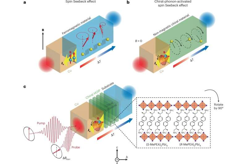
 and experimental setup. Credit: Nature Materials (2023). DOI: 10.1038/s41563-023-01473-9")
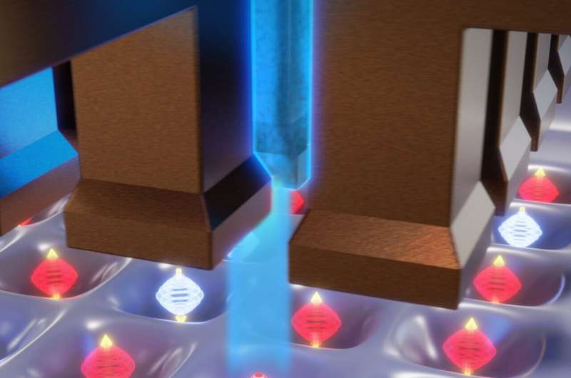
Researchers from North Carolina State University and the University of North Carolina at Chapel Hill used chiral phonons to convert wasted heat into spin information—without needing magnetic materials. The finding could lead to new classes of less expensive, energy-efficient spintronic devices for use in applications ranging from computational memory to power grids.
Spintronic devices are electronic devices that harness the spin of an electron, rather than its charge, to create current used for data storage, communication, and computing. Spin caloritronic devices—so-called because they utilize thermal energy to create spin current—are promising because they can convert waste heat into spin information, which makes them extremely energy efficient. However, current spin caloritronic devices must contain magnetic materials in order to create and control the electron’s spin.
“We used chiral phonons to create a spin current at room temperature without needing magnetic materials,” says Dali Sun, associate professor of physics and member of the Organic and Carbon Electronics Lab (ORaCEL) at North Carolina State University.
“By applying a thermal gradient to a material that contains chiral phonons, you can direct their angular momentum and create and control spin current,” says Jun Liu, associate professor of mechanical and aerospace engineering at NC State and ORaCEL member.
Both Liu and Sun are co-corresponding authors of the research, which appears in Nature Materials.
Chiral phonons are groups of atoms that move in a circular direction when excited by an energy source—in this case, heat. As the phonons move through a material, they propagate that circular motion, or angular momentum, through it. The angular momentum serves as the source of spin, and the chirality dictates the direction of the spin.
“Chiral materials are materials that cannot be superimposed on their mirror image,” Sun says. “Think of your right and left hands—they are chiral. You can’t put a left-handed glove on a right hand, or vice versa. This ‘handedness’ is what allows us to control the spin direction, which is important if you want to use these devices for memory storage.”
The researchers demonstrated chiral phonon-generated spin currents in a two-dimensional layered hybrid organic-inorganic perovskite by using a thermal gradient to introduce heat to the system.
“A gradient is needed because temperature difference in the material—from hot to cold—drives the motion of the chiral phonons through it,” says Liu. “The thermal gradient also allows us to use captured waste heat to generate spin current.”
The researchers hope that the work will lead to spintronic devices that are cheaper to produce and can be used in a wider variety of applications.
“Eliminating the need for magnetism in these devices means you’re opening the door wide in terms of access to potential materials,” Liu says. “And that also means increased cost-effectiveness.”
“Using waste heat rather than electric signals to generate spin current makes the system energy efficient—and the devices can operate at room temperature,” Sun says. “This could lead to a much wider variety of spintronic devices than we currently have available.”
More information: Lifa Zhang, Chiral-phonon-activated spin Seebeck effect, Nature Materials (2023). DOI: 10.1038/s41563-023-01473-9. www.nature.com/articles/s41563-023-01473-9
Journal information: Nature Materials
Provided by North Carolina State University

 which was operated in multi-turn energy recovery mode. Credit: J.-C. Hartung Credit: Schliessmann et al.")
-(5). In a conventional mode, the beam would be dumped at high energy after it has been used for an experiment (6), where the energy stored in the electron beam would be wasted. In the energy recovery mode, the electron beam is instead decelerated (7)-(10) and then dumped at low energy (11). During deceleration, energy is recovered in the cavities of the main linear accelerator. The recovered energy is then recycled by accelerating subsequent electron bunches. By passing the main accelerator twice (multi-turn), higher beam energies can be achieved. Credit: F. Schliessmann et al./Nature Physics. Credit: Schliessmann et al.")
 and valley states (blue and red orbitals). In the presence of a DC voltage (blue glow) an electron can undergo coherent spin-valley oscillation. Image credit: Mike Osadciw.")
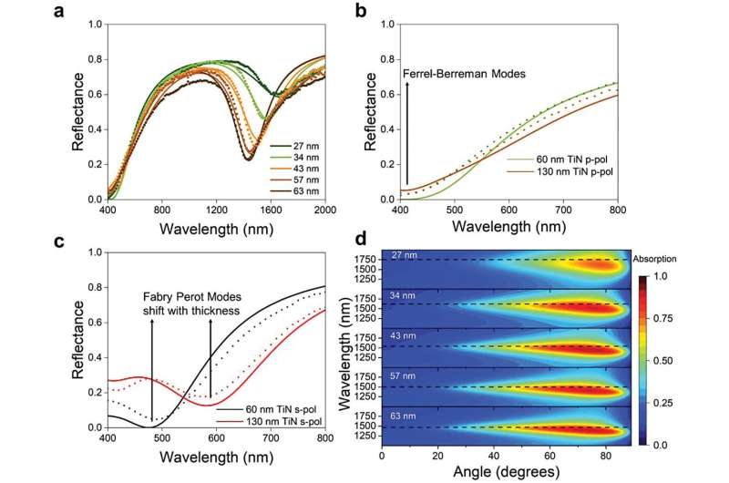
 Reflectance spectrum of the ultra-subwavelength AZO on TiN for p-polarized light. b) Ferrell–Berreman modes for p-polarized and c) Fabry–Pérot modes for s-polarized light on the TiN–AZO films with varying TiN thickness. The solid lines in (a)–(c) are simulation results. The dashed lines are experimental results. d) Angle- and wavelength-dependent absorption spectrum of the AZO films obtained using the TMM method. Credit: Advanced Materials (2022). DOI: 10.1002/adma.202109546")
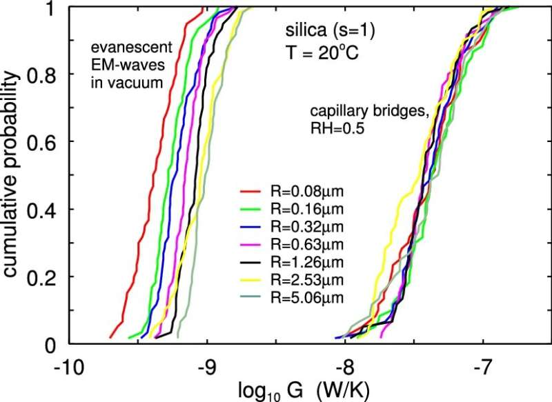
 waves (in vacuum), and due to heat conduction in water capillary bridges. Credit: The European Physical Journal B (2023). DOI: 10.1140/epjb/s10051-023-00483-5")


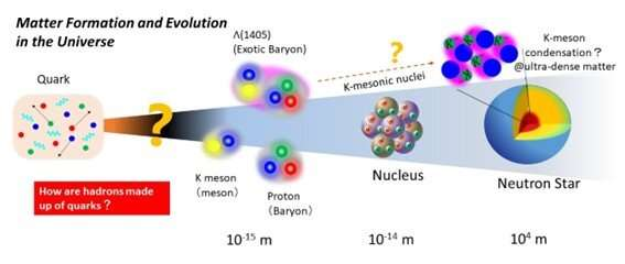
 and a schematic illustration of the evolution of matter. Credit: Hiroyuki Noumi")
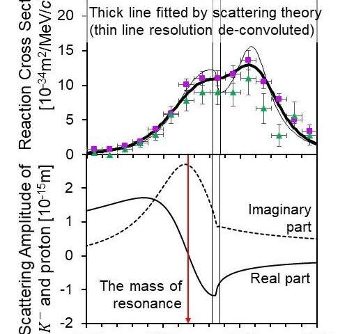 (Top) Measured reaction cross-section. The horizontal axis is the K– and proton collision recoil energy converted into a mass value. Large reaction events occur at mass values lower than the sum of the K– and proton masses, which itself suggests the existence of Λ(1405). The measured data were reproduced by scattering theory (solid lines). (Bottom) Distribution of K– and proton scattering amplitudes. When squared, these correspond to the reaction cross-section, and are generally complex numbers. The calculated values match with the measured data. When the real part (solid line) crosses 0, the value of the imaginary part reaches its maximum value. This is a typical distribution for a resonance state, and determines the complex mass. The arrows indicate the real part. Credit: 2023, Hiroyuki Noumi, Pole position of Λ(1405) measured in d(K^-,n)πΣ reactions, Physics Letters B
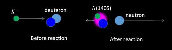 Schematic illustration of the reaction used to synthesize Λ(1405) by fusing a K– (green circle) with a proton (dark blue circle), which takes place inside a deuteron nucleus. Credit: Hiroyuki Noumi
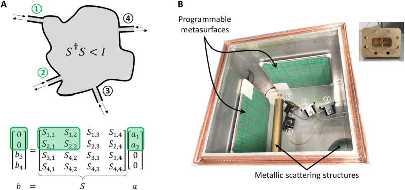
 Generic schematic of a nonunitary scattering system with four attached channels and matrix formalism corresponding to an RSM involving channels 1 and 2 (highlighted in green). (B) Photographic image of the corresponding experimental setup comprising a metallic electrically large scattering enclosure with irregularly shaped metallic scattering structures (top cover removed to show interior), two programmable metasurfaces composed of 152 meta-atoms each, and four waveguide-to-coax adapters to couple four monomodal channels to the system. The inset shows the front view of a waveguide-to-coax adapter. Credit: Science Advances (2023). DOI: 10.1126/sciadv.adf0323")