Study proves a generalization of Bell’s theorem: Quantum correlations are genuinely tripartite and nonlocal

Credit: Marya Kuderska

Quantum theory predicts the existence of so-called tripartite-entangled states, in which three quantum particles are related in a way that has no counterpart in classical physics. Theoretical physicists would like to understand how well new theories, alternatives to quantum theory, might be able to reproduce the behavior of these states.

John Clauser, Alain Aspect and Anton Zeilinger, whose work was recently recognized by the Nobel Committee, have experimentally proven Bell’s theorem, showing that no local hidden-variable alternative to quantum theory can reproduce this behavior. In other words, they showed that quantum correlations are nonlocal.

Researchers at the University of Science and Technology of China, Institute of Photonic Sciences, Università della Svizzera Italiana and Perimeter Institute of Theoretical Physics have recently carried out an experimental study generalizing these findings, by considering new potential theories. Their findings, published in Physical Review Letters, suggest that the correlations achieved by the tripartite-entangled state used in their experiment cannot be explained by an hypothetical theory involving a generalization of bipartite entanglement, called “exotic sources of two particles,” in addition to a local hidden-variable theory.

“The main objective of our study was to prove that the behavior of a three particle quantum source (e.g., a source of three photons) cannot be reproduced by any new hypothetical theory (replacing quantum theory, yet to be discovered) which only involves exotic pairs of two particle described by new physical laws’ and a local hidden variable model,” Marc-Olivier Renou, one of the authors of the paper, told Phys.org.

Gaël Massé, a second author, explains: “To do this, we used the idea contained in the ‘inflation technique,’ invented by Elie Wolfe, one of our coauthor. If we imagine a pair of two particles described by new physical laws, then even if we have no idea how to describe them we can still create a copy of this pair and make all the particles interact together in a new way. While this technique seems elementary, it has often proved to be a very powerful tool to address theoretical abstract concepts.”

Study proves a generalization of bell theorem: quantum correlations are genuinely tripartite nonlocal
Credit: Marya Kuderska

In their paper, the researchers first derived a new device-independent witness that could falsify causal theories with bipartite nonclassical resources. Then, through a lab experiment performed by Huan Cao and Chao Zhang, they showed that some tripartite-entangled state (called the “GHZ state”) could obtain, in practice, correlations that violate this witness.

“Using a high-performance photonic GHZ3 state with fidelities of 0.9741±0.002, we provide a clear experimental violation of that witness by more than 26.3 standard deviations, under the locality and fair sampling assumption,” the team explained in their paper. “We generalize our Letter to the |GHZ4⟩ state, obtaining correlations that cannot be explained by any causal theory limited to tripartite nonclassical common causes assisted with unlimited shared randomness.”

The recent work is a generalization of Bell’s theorem. Its most remarkable achievement is that it reaches beyond what physicists previously thought was possible in constraining potential alternative theories to quantum theory.

Study proves a generalization of bell theorem: quantum correlations are genuinely tripartite nonlocal
Credit: Marya Kuderska

“Bell ruled out the possibility that quantum correlations can be explained by a local hidden variable model (i.e., shared randomness),” Xavier Coiteux-Roy, a coauthor of the study, explains. “We went a bit further, by proving that even if you add ‘bipartite exotic sources’ in your theory, it still doesn’t work. In fact, we generalized the result, showing that if you add tripartite, quadripartite, and other exotic sources, it still doesn’t work. You really need to involve N-partite exotic sources for any N, whatever high it is, as is done by quantum theory.” He concludes, “Note that experiment has imperfections, called loopholes. Realizing an experiment without these loopholes, in particular the post-selection loophole, is a great challenge for experimentalists for the next years.”

Based on their findings, the team concluded that nature’s correlations are genuinely multipartite nonlocal. The experiments they carried out so far allowed them to definitively exclude theories of bipartite and tripartite exotic sources, but they are now thinking of evaluating other alternatives to quantum theory.

“We are now trying to understand how far this idea can go, and how far we can exclude potential alternatives to quantum theory by just looking at concrete experimental results, without assuming that they are explained by quantum theory,” Renou added. “This might eventually allow us to exclude all potential alternatives to quantum theory.”

More information: Huan Cao et al, Experimental Demonstration that No Tripartite-Nonlocal Causal Theory Explains Nature’s Correlations, Physical Review Letters (2022). DOI: 10.1103/PhysRevLett.129.150402

Journal information: Physical Review Letters 

© 2022 Science X Network

Light-analyzing ‘lab on a chip’ opens door to widespread use of portable spectrometers

Spectrometer on a chip. Credit: Oregon State

Scientists including an Oregon State University materials researcher have developed a better tool to measure light, contributing to a field known as optical spectrometry in a way that could improve everything from smartphone cameras to environmental monitoring.

The study, published today in Science, was led by Finland’s Aalto University and resulted in a powerful, ultra-tiny spectrometer that fits on a microchip and is operated using artificial intelligence.

The research involved a comparatively new class of super-thin materials known as two-dimensional semiconductors, and the upshot is a proof of concept for a spectrometer that could be readily incorporated into a variety of technologies—including quality inspection platforms, security sensors, biomedical analyzers and space telescopes.

“We’ve demonstrated a way of building spectrometers that are far more miniature than what is typically used today,” said Ethan Minot, a professor of physics in the OSU College of Science. “Spectrometers measure the strength of light at different wavelengths and are super useful in lots of industries and all fields of science for identifying samples and characterizing materials.”

Traditional spectrometers require bulky optical and mechanical components, whereas the new device could fit on the end of a human hair, Minot said. The new research suggests those components can be replaced with novel semiconductor materials and AI, allowing spectrometers to be dramatically scaled down in size from the current smallest ones, which are about the size of a grape.

“Our spectrometer does not require assembling separate optical and mechanical components or array designs to disperse and filter light,” said Hoon Hahn Yoon, who led the study with Aalto University colleague Zhipei Sun Yoon. “Moreover, it can achieve a high resolution comparable to benchtop systems but in a much smaller package.”

The device is 100% electrically controllable regarding the colors of light it absorbs, which gives it massive potential for scalability and widespread usability, the researchers say.

“Integrating it directly into portable devices such as smartphones and drones could advance our daily lives,” Yoon said. “Imagine that the next generation of our smartphone cameras could be hyperspectral cameras.”

Those hyperspectral cameras could capture and analyze information not just from visible wavelengths but also allow for infrared imaging and analysis.

“It’s exciting that our spectrometer opens up possibilities for all sorts of new everyday gadgets, and instruments to do new science as well,” Minot said.

In medicine, for example, spectrometers are already being tested for their ability to identify subtle changes in human tissue such as the difference between tumors and healthy tissue.

For environmental monitoring, Minot added, spectrometers can detect exactly what kind of pollution is in the air, water or ground, and how much of it is there.

“It would be nice to have low-cost, portable spectrometers doing this work for us,” he said. “And in the educational setting, the hands-on teaching of science concepts would be more effective with inexpensive, compact spectrometers.”

Applications abound as well for science-oriented hobbyists, Minot said.

“If you’re into astronomy, you might be interested in measuring the spectrum of light that you collect with your telescope and having that information identify a star or planet,” he said. “If geology is your hobby, you could identify gemstones by measuring the spectrum of light they absorb.”

Minot thinks that as work with two-dimensional semiconductors progresses, “we’ll be rapidly discovering new ways to use their novel optical and electronic properties.” Research into 2D semiconductors has been going on in earnest for only a dozen years, starting with the study of graphene, carbon arranged in a honeycomb lattice with a thickness of one atom.

“It’s really exciting,” Minot said. “I believe we’ll continue to have interesting breakthroughs by studying two-dimensional semiconductors.”

In addition to Minot, Yoon and Sun, the collaboration included scientists from Shanghai Jiao Tong University, Zhejiang University, Sichuan University, Yonsei University and University of Cambridge, as well as other researchers from Aalto University.

Universal parity quantum computing, a new architecture that overcomes performance limitations

Illustration of the modified LHZ architecture with logical lines. Three- and four-body constraints are represented by light gray triangles and squares between corresponding qubits. Data qubits with single logical indices are added as an additional row at the bottom of the architecture to allow direct access to logical Rz rotations. Colored lines connect all qubits whose labels contain the same logical index. Logical Rx rotations can be realized with chains of cnot gates along the corresponding line. Credit: Physical Review Letters (2022). DOI: 10.1103/PhysRevLett.129.180503

The computing power of quantum machines is currently still very low. Increasing performance is a major challenge. Physicists at the University of Innsbruck, Austria, now present a new architecture for a universal quantum computer that overcomes such limitations and could be the basis of the next generation of quantum computers soon.

Quantum bits (qubits) in a quantum computer serve as a computing unit and memory at the same time. Because quantum information cannot be copied, it cannot be stored in memory as in a classical computer. Due to this limitation, all qubits in a quantum computer must be able to interact with each other.

This is currently still a major challenge for building powerful quantum computers. In 2015, theoretical physicist Wolfgang Lechner, together with Philipp Hauke and Peter Zoller, addressed this difficulty and proposed a new architecture for a quantum computer, now named LHZ architecture after the authors.

“This architecture was originally designed for optimization problems,” says Wolfgang Lechner of the Department of Theoretical Physics at the University of Innsbruck, Austria. “In the process, we reduced the architecture to a minimum in order to solve these optimization problems as efficiently as possible.”

The physical qubits in this architecture do not represent individual bits, but encode the relative coordination between the bits. “This means that not all qubits have to interact with each other anymore,” explains Wolfgang Lechner. With his team, he has now shown that this parity concept is also suitable for a universal quantum computer.

Complex operations are simplified

Parity computers can perform operations between two or more qubits on a single qubit. “Existing quantum computers already implement such operations very well on a small scale,” Michael Fellner from Wolfgang Lechner’s team explains. “However, as the number of qubits increases, it becomes more and more complex to implement these gate operations.”

In two publications in Physical Review Letters and Physical Review A, the Innsbruck scientists now show that parity computers can, for example, perform quantum Fourier transformations—a fundamental building block of many quantum algorithms—with significantly fewer computation steps and thus more quickly. “The high parallelism of our architecture means that, for example, the well-known Shor algorithm for factoring numbers can be executed very efficiently,” Fellner explains.

Two-stage error correction

The new concept also offers hardware-efficient error correction. Because quantum systems are very sensitive to disturbances, quantum computers must correct errors continuously. Significant resources must be devoted to protecting quantum information, which greatly increases the number of qubits required. “Our model operates with a two-stage error correction, one type of error (bit flip error or phase error) is prevented by the hardware used,” write Anette Messinger and Kilian Ender, also members of the Innsbruck research team.

There are already initial experimental approaches for this on different platforms. “The other type of error can be detected and corrected via the software,” Messinger and Ender say. This would allow a next generation of universal quantum computers to be realized with manageable effort.

The spin-off company ParityQC, co-founded by Wolfgang Lechner and Magdalena Hauser, is already working in Innsbruck with partners from science and industry on possible implementations of the new model.

Electrons with Planckian scattering in strange metals follow standard rules of orbital motion in a magnet

The 100-tesla magnet system at the National Laboratory for Intense Magnetic Fields in Toulouse, France. Credit: Nanda Gonzague.

Strange metals, or non-Fermi liquids, are distinct states of matter that have been observed in different quantum materials, including cuprate superconductors. These states are characterized by unusual conductive properties, such as a resistivity that is linearly associated with temperature (T-linear).

In the strange metal phase of matter, electrons undergo what is known as “Planckian dissipation,” a high scattering rate that linearly increases as the temperature rises. This T-linear, strong electron scattering is anomalous for metals, which typically present a quadratic temperature dependence (T2), as predicted by the standard theory of metals.

Researchers at Université de Sherbrooke in Canada, Laboratoire National des Champs Magnétiques Intenses in France, and other institutes worldwide have recently carried out a study exploring the possibility that the resistivity of strange metals is not only associated with temperature, but also with an applied magnetic field. This magnetic field linearity had been previously observed in some cuprates and pnictides, with some physicists suggesting that it could also be linked to Planckian dissipation.

The researchers carried out their experiments on two specific cuprate strange metals, namely Nd0.4La1.6−xSrxCuO4 and La2−xSrxCuO4. Their findings, published in Nature Physics, suggest that the resistivity of these two strange metals is consistent with the predictions of the standard Boltzmann theory of electron motion in a magnetic field in all ways, highlighting no anomaly associated with Planckian dissipation.

“We wanted to investigate the field dependence of Planckian scattering rate in the strange metal phase of cuprate superconductors, in particular in NdLSCO, that its scattering rate was previously measured with Angle Dependence Magnetoresistance (ADMR) experiments,” Amirreza Ataei, one of the researchers who carried out the study, told Phys.org. “In this material, due to a relatively low critical temperature, Tc, we had access to one of the largest measured ranges of B-linear resistivity and were able to reproduce the magnetoresistance over this magnetic field range using the standard Boltzmann theory.”

Study shows that electrons with Planckian scattering in strange metals follow standard rules of orbital motion in a magn
The sample holder that was used for high field measurements at Toulouse. The length of the black single crystal sample is less than 2 mm, the contacts were made with silver epoxy and 25 micrometer wires, and the sample is mounted on a sapphire plate Credit: Ataei M.Sc. thesis https://savoirs.usherbrooke.ca/handle/11143/15285

A key objective of the recent work by Ataei and his colleagues was to determine whether the in-plane magnetoresistance in the strange metal phase of namely Nd0.4La1.6−xSrxCuO4 and La2−xSrxCuOwas anomalous in instances where the magnetic field and electric current were in parallel. Ultimately, the measurements they collected suggest that it was not.

“We expect our findings to have a big impact in the field of Planckian dissipation, a major mystery in condensed-matter physics with intriguing connections to the physics of black holes,” Ataei explained. “We show that this enigmatic phenomenon is insensitive to magnetic field, up to 85 T, one of the highest achievable magnetic fields in the world.”

Study shows that electrons with Planckian scattering in strange metals follow standard rules of orbital motion in a magn
Louis Taillefer, Cyril Proust and Seyed Amirreza Ataei. Credit: Michel Caron – UdeS.

Overall, the results gathered by this team of researchers would seem to challenge the hypothesis that the linear dependence of resistivity on a magnetic field observed in some strange metals is associated with Planckian dissipation. In contrast, their experimental data suggests that Planckian dissipation is only anomalous in its temperature dependence, while its field dependence is aligned with standard theoretical predictions.

“We now plan to extend the scope of this research to different quantum materials in the strange metal phase or in its proximity,” Ataei added.

New hybrid structures could pave the way to more stable quantum computers

New hybrid structures could pave the way to more stable quantum computers
RHEED patterns during MBE growth. (a) Bilayer graphene terminated 6H-SiC(0001) substrate. (b) Monolayer NbSe2 film grown on bilayer graphene. (c) 5 QL Bi2Se3/monolayer NbSe2 heterostructure grown on bilayer graphene. Credit: Nature Materials (2022). DOI: 10.1038/s41563-022-01386-z

A new way to combine two materials with special electrical properties—a monolayer superconductor and a topological insulator—provides the best platform to date to explore an unusual form of superconductivity called topological superconductivity. The combination could provide the basis for topological quantum computers that are more stable than their traditional counterparts.

Superconductors—used in powerful magnets, digital circuits, and imaging devices—allow the electric current to pass without resistance, while topological insulators are thin films only a few atoms thick that restrict the movement of electrons to their edges, which can result in unique properties. A team led by researchers at Penn State describe how they have paired the two materials in a paper appearing Oct. 27 in the journal Nature Materials.

“The future of quantum computing depends on a kind of material that we call a topological superconductor, which can be formed by combining a topological insulator with a superconductor, but the actual process of combining these two materials is challenging,” said Cui-Zu Chang, Henry W. Knerr Early Career Professor and Associate Professor of Physics at Penn State and leader of the research team.

“In this study, we used a technique called molecular beam epitaxy to synthesize both topological insulator and superconductor films and create a two-dimensional heterostructure that is an excellent platform to explore the phenomenon of topological superconductivity.”

In previous experiments to combine the two materials, the superconductivity in thin films usually disappears once a topological insulator layer is grown on top. Physicists have been able to add a topological insulator film onto a three-dimensional “bulk” superconductor and retain the properties of both materials.

However, applications for topological superconductors, such as chips with low power consumption inside quantum computers or smartphones, would need to be two-dimensional.

In this paper, the research team stacked a topological insulator film made of bismuth selenide (Bi2Se3) with different thicknesses on a superconductor film made of monolayer niobium diselenide (NbSe2), resulting in a two-dimensional end-product. By synthesizing the heterostructures at very lower temperature, the team was able to retain both the topological and superconducting properties.

“In superconductors, electrons form ‘Cooper pairs’ and can flow with zero resistance, but a strong magnetic field can break those pairs,” said Hemian Yi, a postdoctoral scholar in the Chang Research Group at Penn State and the first author of the paper.

“The monolayer superconductor film we used is known for its ‘Ising-type superconductivity,’ which means that the Cooper pairs are very robust against the in-plane magnetic fields. We would also expect the topological superconducting phase formed in our heterostructures to be robust in this way.”

By subtly adjusting the thickness of the topological insulator, the researchers found that the heterostructure shifted from Ising-type superconductivity—where the electron spin is perpendicular to the film—to another kind of superconductivity called “Rashba-type superconductivity”—where the electron spin is parallel to the film.

This phenomenon is also observed in the researchers’ theoretical calculations and simulations.

This heterostructure could also be a good platform for the exploration of Majorana fermions, an elusive particle that would be a major contributor to making a topological quantum computer more stable than its predecessors.

“This is an excellent platform for the exploration of topological superconductors, and we are hopeful that we will find evidence of topological superconductivity in our continuing work,” said Chang. “Once we have solid evidence of topological superconductivity and demonstrate Majorana physics, then this type of system could be adapted for quantum computing and other applications.”

A faster way to find and study topological materials

Data structure and model architecture.(a) A schematic of the full XANES spectrum for arepresentative sample in the dataset, showing the signatures from di↵erent absorbing elements on an absolute energyscale. For a given material, the inputs to the NN classifier consist of one-hot encoded atom types (left) and XANESspectra (right) for all absorbing atoms. (b) Schematic of the neural network architecture predicting the (binary)topological class using spectral and atom-type inputs. Spectral and atom-type inputs are individually embedded byfully-connected layers before performing a direct product between corresponding spectral and atomic channels.These composite features are aggregated for a given material and passed to a final fully-connected block to predictthe topological class. Credit: Advanced Materials (2022). DOI: 10.1002/adma.202204113

Topological materials, an exotic class of materials whose surfaces exhibit different electrical or functional properties than their interiors, have been a hot area of research since their experimental realization in 2007—a finding that sparked further research and precipitated a Nobel Prize in Physics in 2016. These materials are thought to have great potential in a variety of fields, and might someday be used in ultraefficient electronic or optical devices, or key components of quantum computers.

But there are many thousands of compounds that may theoretically have topological characteristics, and synthesizing and testing even one such material to determine its topological properties can take months of experiments and analysis. Now a team of researchers at MIT and elsewhere have come up with a new approach that can rapidly screen candidate materials and determine with more than 90 percent accuracy whether they are topological.

Using this new method, the researchers have produced a list candidate materials. A few of these were already known to have topological properties, but the rest are newly predicted by this approach.

The findings are reported in the journal Advanced Materials in a paper by Mingda Li, the Class ’47 Career Development Professor at MIT, graduate students (and twin sisters) Nina Andrejevic at MIT and Jovana Andrejevic at Harvard University, and seven others at MIT, Harvard, Princeton University, and Argonne National Laboratory.

Topological materials are named after a branch of mathematics that describes shapes based on their invariant characteristics, which persist no matter how much an object is continuously stretched or squeezed out of its original shape. Topological materials, similarly, have properties that remain constant despite changes in their conditions, such as external perturbations or impurities.

There are several varieties of topological materials, including semiconductors, conductors, and semimetals, among others. Initially, it was thought that there were only a handful of such materials, but recent theory and calculations have predicted that in fact thousands of different compounds may have at least some topological characteristics. The hard part is figuring out experimentally which compounds may be topological.

Applications for such materials span a wide range, including devices that could perform computational and data storage functions similarly to silicon-based devices but with far less energy loss, or devices to harvest electricity efficiently from waste heat, for example in thermal power plants or in electronic devices. Topological materials can also have superconducting properties, which could potentially be used to build the quantum bits for topological quantum computers.

But all of this relies on developing or discovering the right materials. “To study a topological material, you first have to confirm whether the material is topological or not,” Li says, “and that part is a hard problem to solve in the traditional way.”

A method called density functional theory is used to perform initial calculations, which then need to be followed with complex experiments that require cleaving a piece of the material to atomic-level flatness and probing it with instruments under high-vacuum conditions.

“Most materials cannot even be measured due to various technical difficulties,” Nina Andrejevic says. But for those that can, the process can take a long time. “It’s a really painstaking procedure,” she says.

Sensitivity to spectral energy resolution. The overall recall, precision, and F1 scores for (a) topological and (b) trivial examples as a function of the energy interval E between sampled points of the XANES spectra. Scores are presented for both the SVM and NN models, with scores from the atom-type only models (SVM-type and NN-type) shown as a reference by the dotted lines. Spectra were resampled at lower resolutions by computing their average values over length E intervals along the energy axis for varied E. To maintain the same number of neurons across all resolutions, the averaged values were copied by the number of original samples within each interval such that all spectral inputs have length 200. Credit: Advanced Materials (2022). DOI: 10.1002/adma.202204113


Whereas the traditional approach relies on measuring the material’s photoemissions or tunneling electrons, Li explains, the new technique he and his team developed relies on absorption, specifically, the way the material absorbs X-rays.

Unlike the expensive apparatus needed for the conventional tests, X-ray absorption spectrometers are readily available and can operate at room temperature and atmospheric pressure, with no vacuum needed. Such measurements are widely conducted in biology, chemistry, battery research, and many other applications, but they had not previously been applied to identifying topological quantum materials.

X-ray absorption spectroscopy provides characteristic spectral data from a given sample of material. The next challenge is to interpret that data and how it relates to the topological properties. For that, the team turned to a machine-learning model, feeding in a collection of data on the X-ray absorption spectra of known topological and nontopological materials, and training the model to find the patterns that relate the two. And it did indeed find such correlations.

“Surprisingly, this approach was over 90 percent accurate when tested on more than 1500 known materials,” Nina Andrejevic says, adding that the predictions take only seconds. “This is an exciting result given the complexity of the conventional process.”

Though the model works, as with many results from machine learning, researchers don’t yet know exactly why it works or what the underlying mechanism is that links the X-ray absorption to the topological properties.

“While the learned function relating X-ray spectra to topology is complex, the result may suggest that certain attributes the measurement is sensitive to, such as local atomic structures, are key topological indicators,” Jovana Andrejevic says.

The team has used the model to construct a periodic table that displays the model’s overall accuracy on compounds made from each of the elements. It serves as a tool to help researchers home in on families of compounds that may offer the right characteristics for a given application.

The researchers have also produced a preliminary study of compounds that they have used this X-ray method on, without advance knowledge of their topological status, and compiled a list of 100 promising candidate materials—a few of which were already known to be topological.

“This work represents one of the first uses of machine learning to understand what experiments are trying to tell us about complex materials,” says Joel Moore, the Chern-Simons Professor of Physics at the University of California at Berkeley, who was not associated with this research.

“Many kinds of topological materials are well-understood theoretically in principle, but finding material candidates and verifying that they have the right topology of their bands can be a challenge. Machine learning seems to offer a new way to address this challenge: Even experimental data whose meaning is not immediately obvious to a human can be analyzed by the algorithm, and I am excited to see what new materials will result from this way of looking.”

Anatoly Frenkel, a professor in the Department of Materials Science and Chemical Engineering at Stony Brook University and a senior chemist at Brookhaven National Laboratory, further commented that “it was a really nice idea to consider that the X-ray absorption spectrum may hold a key to the topological character in the measured sample.”

How do you solve a problem like a proton? Smash it, then build it back with machine learning

Looking into the HERA tunnel: Berkeley Lab scientists have developed new machine learning algorithms to accelerate the analysis of data collected decades ago by HERA, the world’s most powerful electron-proton collider that ran at the DESY national research center in Germany from 1992 to 2007. Credit: DESY

Protons are tiny yet they carry a lot of heft. They inhabit the center of every atom in the universe and play a critical role in one of the strongest forces in nature.

And yet, protons have a down-to-earth side, too.

Like most particles, protons have spin that act like tiny magnets. Flipping a proton’s spin or polarity may sound like science fiction, but it is the basis of technological breakthroughs that have become essential to our daily lives, such as magnetic resonance imaging (MRI), the invaluable medical diagnostics tool.

Despite such advancements, the proton’s inner workings remain a mystery.

“Basically everything around you exists because of protons—and yet we still don’t understand everything about them. One huge puzzle that physicists want to solve is the proton’s spin,” said Ben Nachman, a physicist who leads the Machine Learning Group in the Physics Division at the Department of Energy’s Lawrence Berkeley National Laboratory (Berkeley Lab).

Understanding how and why protons spin could lead to technological advancements we can’t even imagine today, and help us understand the strong force, a fundamental property that gives all protons and therefore atoms mass.

But it’s not such an easy problem to solve. For one, you can’t exactly pick up a proton and place it in a petri dish: Protons are unfathomably small—their radius is a hair shy of one quadrillionth of a meter, and visible light passes right through them. What’s more, you can’t even observe their insides with the world’s most powerful electron microscopes.

Recent work by Nachman and his team could bring us closer to solving this perplexing proton puzzle.

As a member of the H1 Collaboration—an international group that now includes 150 scientists from 50 institutes and 15 countries, and is based at the DESY national research center in Germany—Nachman has been developing new machine learning algorithms to accelerate the analysis of data collected decades ago by HERA, the world’s most powerful electron-proton collider that ran at DESY from 1992 to 2007.

HERA—a ring 4 miles in circumference—worked like a giant microscope that accelerated both electrons and protons to nearly the speed of light. The particles were collided head-on, which could scatter a proton into its constituent parts: quarks and gluons.

Scientists at HERA took measurements of the particle debris cascading from these electron-proton collisions, what physicists call “deep inelastic scattering,” through sophisticated cameras called particle detectors, one of which was the H1 detector.

Unfolding secrets of the strong force

The H1 stopped collecting data in 2007, the year HERA was decommissioned. Today, the H1 Collaboration is still analyzing the data and publishing results in scientific journals.

The HERA electron-proton collider accelerated both electrons and protons to nearly the speed of light. The particles were collided head-on, which could scatter a proton into its constituent parts: quarks (shown as green and purple balls in the illustration above) and gluons (illustrated as black coils). Credit: DESY


It can take a year or more when using conventional computational techniques to measure quantities related to proton structure and the strong force, such as how many particles are produced when a proton collides with an electron.

And if a researcher wants to examine a different quantity, such as how fast particles are flying in the wake of a quark-gluon jet stream, they would have to start the long computational process all over again, and wait yet another year.

A new machine learning tool called OmniFold—which Nachman co-developed—can simultaneously measure many quantities at once, thereby reducing the amount of time to run an analysis from years to minutes.

OmniFold does this by using neural networks at once to combine computer simulations with data. (A neural network is a machine learning tool that processes complex data that is impossible for scientists to do manually.)

Nachman and his team applied OmniFold to H1 experimental data for the first time in a June issue of the journal Physical Review Letters and more recently at the 2022 Deep Inelastic Scattering (DIS) Conference.

To develop OmniFold and test its robustness against H1 data, Nachman and Vinicius Mikuni, a postdoctoral researcher in the Data and Analytics Services (DAS) group at Berkeley Lab’s National Energy Research Scientific Computing Center (NERSC) and a NERSC Exascale Science Applications Program for Learning fellow, needed a supercomputer with a lot of powerful GPUs (graphics processing units), Nachman said.

Coincidentally, Perlmutter, a new supercomputer designed to support simulation, data analytics, and artificial intelligence experiments requiring multiple GPUs at a time, had just opened up in the summer of 2021 for an “early science phase,” allowing scientists to test the system on real data. (The Perlmutter supercomputer is named for the Berkeley Lab cosmologist and Nobel laureate Saul Perlmutter.)

“Because the Perlmutter supercomputer allowed us to use 128 GPUs simultaneously, we were able to run all the steps of the analysis, from data processing to the derivation of the results, in less than a week instead of months. This improvement allows us to quickly optimize the neural networks we trained and to achieve a more precise result for the observables we measured,” said Mikuni, who is also a member of the H1 Collaboration.

A central task in these measurements is accounting for detector distortions. The H1 detector, like a watchful guard standing sentry at the entrance of a sold-out concert arena, monitors particles as they fly through it. One source of measurement errors happens when particles fly around the detector rather than through it, for example—sort of like a ticketless concert goer jumping over an unmonitored fence rather than entering through the ticketed security gate.

Correcting for all distortions simultaneously had not been possible due to limited computational methods available at the time. “Our understanding of subatomic physics and data analysis techniques have advanced significantly since 2007, and so today, scientists can use new insights to analyze the H1 data,” Nachman said.

Scientists today have a renewed interest in HERA’s particle experiments, as they hope to use the data—and more precise computer simulations informed by tools like OmniFold—to aid in the analysis of results from future electron-proton experiments, such as at the Department of Energy’s next-generation Electron-Ion Collider (EIC).

The EIC—to be built at Brookhaven National Laboratory in partnership with the Thomas Jefferson National Accelerator Facility—will be a powerful and versatile new machine capable of colliding high-energy beams of polarized electrons with a wide range of ions (or charged atoms) across many energies, including polarized protons and some polarized ions.

“It’s exciting to think that our method could one day help scientists answer questions that still remain about the strong force,” Nachman said.

“Even though this work might not lead to practical applications in the near term, understanding the building blocks of nature is why we’re here—to seek the ultimate truth. These are steps to understanding at the most basic level what everything is made of. That is what drives me. If we don’t do the research now, we will never know what exciting new technological advances we’ll get to benefit future societies.”

With scanning ultrafast electron microscopy, researchers unveil hot photocarrier transport properties of cubic boron

In a study that confirms its promise as the next-generation semiconductor material, UC Santa Barbara researchers have directly visualized the photocarrier transport properties of cubic boron arsenide single crystals.

“We were able to visualize how the charge moves in our sample,” said Bolin Liao, an assistant professor of mechanical engineering in the College of Engineering. Using the only scanning ultrafast electron microscopy (SUEM) setup in operation at a U.S. university, he and his team were able to make “movies” of the generation and transport processes of a photoexcited charge in this relatively little-studied III-V semiconductor material, which has recently been recognized as having extraordinary electrical and thermal properties. In the process, they found another beneficial property that adds to the material’s potential as the next great semiconductor.

Their research, conducted in collaboration with physics professor Zhifeng Ren’s group at the University of Houston, who specialize in fabricating high-quality single crystals of cubic boron arsenide, appears in the journal Matter.

‘Ringing the bell’

Boron arsenide is being eyed as a potential candidate to replace silicon, the computer world’s staple semiconductor material, due to its promising performance. For one thing, with an improved charge mobility over silicon, it easily conducts current (electrons and their positively charged counterpart, “holes”). However, unlike silicon, it also conducts heat with ease.

“This material actually has 10 times higher thermal conductivity than silicon,” Liao said. This heat conducting—and releasing—ability is particularly important as electronic components become smaller and more densely packed, and pooled heat threatens the devices’ performance, he explained.

“As your cellphones become more powerful, you want to be able to dissipate the heat, otherwise you have efficiency and safety issues,” he said. “Thermal management has been a challenge for a lot of microelectronic devices.”

What gives rise to the high thermal conductivity of this material, it turns out, can also lead to interesting transport properties of photocarriers, which are the charges excited by light, for example, in a solar cell. If experimentally verified, this would indicate that cubic boron arsenide can also be a promising material for photovoltaic and light detection applications. Direct measurement of photocarrier transport in cubic boron arsenide, however, has been challenging due to the small size of available high-quality samples.

The research team’s study combines two feats: The crystal growth skills of the University of Houston team, and the imaging prowess at UC Santa Barbara. Combining the abilities of the scanning electron microscope and femtosecond ultrafast lasers, the UCSB team built what is essentially an extremely fast, exceptionally high-resolution camera.

“Electron microscopes have very good spatial resolution—they can resolve single atoms with their sub-nanometer spatial resolution—but they’re typically very slow,” Liao said, noting this makes them excellent for capturing static images.

“With our technique, we couple this very high spatial resolution with an ultrafast laser, which acts as a very fast shutter, for extremely high time resolution,” Liao continued. “We’re talking about one picosecond—a millionth of a millionth of a second. So we can make movies of these microscopic energy and charge transport processes.” Originally invented at Caltech, the method was further developed and improved at UCSB from scratch and now is the only operational SUEM setup at an American university.

“What happens is that we have one pulse of this laser that excites the sample,” explained graduate student researcher Usama Choudhry, the lead author of the Matter paper. “You can think of it like ringing a bell; it’s a loud noise that slowly diminishes over time.” As they “ring the bell,” he explained, a second laser pulse is focused onto a photocathode (“electron gun”) to generate a short electron pulse to image the sample. They then scan the electron pulse over time to gain a full picture of the ring. “Just by taking a lot of these scans, you can get a movie of how the electrons and holes get excited and eventually go back to normal,” he said.

Among the things they observed while exciting their sample and watching the electrons return to their original state is how long the “hot” electrons persist.

“We found, surprisingly, the ‘hot’ electrons excited by light in this material can persist for much longer times than in conventional semiconductors,” Liao said. These “hot” carriers were seen to persist for more that 200 picoseconds, a property that is related to the same feature that is responsible for the material’s high thermal conductivity. This ability to host “hot” electrons for significantly longer amounts of time has important implications.

“For example, when you excite the electrons in a typical solar cell with light, not every electron has the same amount of energy,” Choudhry explained. “The high-energy electrons have a very short lifetime, and the low-energy electrons have a very long lifetime.” When it comes to harvesting the energy from a typical solar cell, he continued, only the low-energy electrons are efficiently being collected; the high-energy ones tend to lose their energy rapidly as heat. Because of the persistence of the high-energy carriers, if this material was used as a solar cell, more energy could efficiently be harvested from it.

With boron arsenide beating silicon in three relevant areas—charge mobility, thermal conductivity and hot photocarrier transport time—it has the potential to become the electronics world’s next state-of-the-art material. However, it still faces significant hurdles—fabrication of high-quality crystals in large quantities—before it can compete with silicon, enormous amounts of which can be manufactured relatively cheaply and with high quality. But Liao doesn’t see too much of a problem.

“Silicon is now routinely available because of years of investment; people started developing silicon around the 1930s and ’40s,” he said. “I think once people recognize the potential of this material, there will be more effort put into finding ways to grow and use it. UCSB is actually uniquely positioned for this challenge with strong expertise in semiconductor development.”

New data transmission record set using a single laser and a single optical chip

optical chip
Credit: Unsplash/CC0 Public Domain

An international group of researchers from Technical University of Denmark (DTU) and Chalmers University of Technology in Gothenburg, Sweden have achieved dizzying data transmission speeds and are the first in the world to transmit more than 1 petabit per second (Pbit/s) using only a single laser and a single optical chip.

1 petabit corresponds to 1 million gigabits.

In the experiment, the researchers succeeded in transmitting 1.8 Pbit/s, which corresponds to twice the total global Internet traffic. And only carried by the light from one optical source. The light source is a custom-designed optical chip, which can use the light from a single infrared laser to create a rainbow spectrum of many colors, i.e., many frequencies. Thus, the one frequency (color) of a single laser can be multiplied into hundreds of frequencies (colors) in a single chip.

All the colors are fixed at a specific frequency distance from each other—just like the teeth on a comb—which is why it is called a frequency comb. Each color (or frequency) can then be isolated and used to imprint data. The frequencies can then be reassembled and sent over an optical fiber, thus transmitting data. Even a huge volume of data, as the researchers have discovered.

One single laser can replace thousands

The experimental demonstration showed that a single chip could easily carry 1.8 Pbit/s, which—with contemporary state-of-the-art commercial equipment—would otherwise require more than 1,000 lasers.

Victor Torres Company, professor at Chalmers University of Technology, is head of the research group that has developed and manufactured the chip.

“What is special about this chip is that it produces a frequency comb with ideal characteristics for fiber-optical communications—it has high optical power and covers a broad bandwidth within the spectral region that is interesting for advanced optical communications,” says Victor Torres Company.

Interestingly enough, the chip was not optimized for this particular application.

“In fact, some of the characteristic parameters were achieved by coincidence and not by design,” says Victor Torres Company. “However, with efforts in my team, we are now capable to reverse engineer the process and achieve with high reproducibility microcombs for target applications in telecommunications.”

Enormous potential for scaling

In addition, the researchers created a computational model to examine theoretically the fundamental potential for data transmission with a single chip identical to the one used in the experiment. The calculations showed enormous potential for scaling up the solution.

Professor Leif Katsuo Oxenløwe, Head of the Center of Excellence for Silicon Photonics for Optical Communications (SPOC) at DTU, says:

“Our calculations show that—with the single chip made by Chalmers University of Technology, and a single laser—we will be able to transmit up to 100 Pbit/s. The reason for this is that our solution is scalable—both in terms of creating many frequencies and in terms of splitting the frequency comb into many spatial copies and then optically amplifying them, and using them as parallel sources with which we can transmit data. Although the comb copies must be amplified, we do not lose the qualities of the comb, which we utilize for spectrally efficient data transmission.”

This is how you pack light with data

Packing light with data is known as modulation. Here, the wave properties of light are utilized such as:

  • Amplitude (the height/strength of the waves)
  • Phase (the “rhythm” of the waves, where it is possible to make a shift so that a wave arrives either a little earlier or a little later than expected)
  • Polarization (the directions in which the waves spread).

By changing these properties, you create signals. The signals can be translated into either ones or zeros—and thus utilized as data signals.

Reduces Internet power consumption

The researchers’ solution bodes well for the future power consumption of the Internet.

“In other words, our solution provides a potential for replacing hundreds of thousands of the lasers located at Internet hubs and data centers, all of which guzzle power and generate heat. We have an opportunity to contribute to achieving an Internet that leaves a smaller climate footprint,” says Leif Katsuo Oxenløwe.

Even though the researchers have broken the petabit barrier for a single laser source and a single chip in their demonstration, there is still some development work ahead before the solution can be implemented in our current communication systems, according to Leif Katsuo Oxenløwe.

“All over the world, work is being done to integrate the laser source in the optical chip, and we’re working on that as well. The more components we can integrate in the chip, the more efficient the whole transmitter will be, i.e., laser, comb-creating chip, data modulators, and any amplifier elements. It will be an extremely efficient optical transmitter of data signals,” says Leif Katsuo Oxenløwe.

The research is published in Nature Photonics.

Navigating when GPS goes dark

Navigating when GPS goes dark
Cross-sectional renderings of the LPAI sensor head. a, Horizontal cross-section showing the cooling-beam and atom-detection channels with fixed optical components. The cooling-channel light is delivered to the sensor head via a polarization maintaining (PM) 
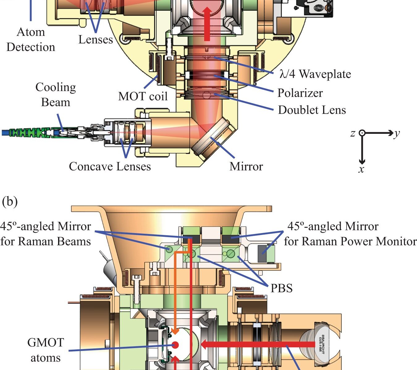
fiber from which a large collimated Gaussian beam (D1/e2≈28mm) is used for cooling. The beam is truncated to ≈ 19 mm-diameter through the fused silica viewport in the compact LPAI sensor head. The light then passes through a polarizer and a λ/4 waveplate before illuminating the grating chip. The GMOT atoms (solid red circle) form ≈ 3.5 mm from the grating surface. The atom-detection channel was designed to measure atomic fluorescence through a multimode-fiber-coupled avalanche photodiode (APD) module. b, Vertical cross-section of the sensor head showing the designed beam paths for Doppler-sensitive Raman. Cross-linearly-polarized Raman beams are launched from the same PM fiber and the two components are split by a polarizing beam splitter (PBS). Fixed optics route the Raman beams to the GMOT atoms (solid red circle) with opposite directions. Credit: Nature Communications (2022). DOI: 10.1038/s41467-022-31410-4

Words like “tough” or “rugged” are rarely associated with a quantum inertial sensor. The remarkable scientific instrument can measure motion a thousand times more accurately than the devices that help navigate today’s missiles, aircraft and drones. But its delicate, table-sized array of components that includes a complex laser and vacuum system has largely kept the technology grounded and confined to the controlled settings of a lab.

Jongmin Lee wants to change that.

The atomic physicist is part of a team at Sandia that envisions quantum inertial sensors as revolutionary, onboard navigational aids. If the team can reengineer the sensor into a compact, rugged device, the technology could safely guide vehicles where GPS signals are jammed or lost.

In a major milestone toward realizing their vision, the team has successfully built a cold-atom interferometer, a core component of quantum sensors, designed to be much smaller and tougher than typical lab setups. The team describes their prototype in the academic journal Nature Communications, showing how to integrate several normally separated components into a single monolithic structure. In doing so, they reduced the key components of a system that existed on a large optical table down to a sturdy package roughly the size of a shoebox.

“Very high sensitivity has been demonstrated in the lab, but the practical matters are, for real-world application, that people need to shrink down the size, weight and power, and then overcome various issues in a dynamic environment,” Jongmin said.

The paper also describes a roadmap for further miniaturizing the system using technologies under development.

The prototype, funded by Sandia’s Laboratory Directed Research and Development program, demonstrates significant strides toward moving advanced navigation tech out of the lab and into vehicles on the ground, underground, in the air and even in space.

Navigating when GPS goes dark
Concept of the compact light-pulse atom interferometer (LPAI) for high-dynamic conditions. a 3D rendering of the compact LPAI sensor head with fixed optical components and reliable optomechanical design. b Picture of the steady-state GMOT atoms in the sensor head.. Credit: Nature Communications (2022). DOI: 10.1038/s41467-022-31410-4

Ultrasensitive measurements drive navigational power

As a jet does a barrel roll through the sky, current onboard navigation tech can measure the aircraft’s tilts and turns and accelerations to calculate its position without GPS, for a time. Small measurement errors gradually push a vehicle off course unless it periodically syncs with the satellites, Jongmin said.

Quantum sensing would operate in the same way, but the much better accuracy would mean onboard navigation wouldn’t need to cross-check its calculations as often, reducing reliance on satellite systems.

Roger Ding, a postdoctoral researcher who worked on the project, said, “In principle, there are no manufacturing variations and calibrations,” compared to conventional sensors that can change over time and need to be recalibrated.

Aaron Ison, the lead engineer on the project, said to prepare the atom interferometer for a dynamic environment, he and his team used materials proven in extreme environments. Additionally, parts that are normally separate and freestanding were integrated together and fixed in place or were built with manual lockout mechanisms.

“A monolithic structure having as few bolted interfaces as possible was key to creating a more rugged atom interferometer structure,” Aaron said.

Furthermore, the team used industry-standard calculations called finite element analysis to predict that any deformation of the system in conventional environments would fall within required allowances. Sandia has not conducted mechanical stress tests or field tests on the new design, so further research is needed to measure the device’s strength.

“The overall small, compact design naturally leads towards a stiffer more robust structure,” Aaron said.

Navigating when GPS goes dark
Sandia atomic physicist Jongmin Lee examines the sensor head of a cold-atom interferometer that could help vehicles stay on course where GPS is unavailable. Credit: Bret Latter

Photonics light the way to a more miniaturized system

Most modern atom interferometry experiments use a system of lasers mounted to a large optical table for stability reasons, Roger said. Sandia’s device is comparatively compact, but the team has already come up with further design improvements to make the quantum sensors much smaller using integrated photonic technologies.

“There are tens to hundreds of elements that can be placed on a chip smaller than a penny,” said Peter Schwindt, the principal investigator on the project and an expert in quantum sensing.

Photonic devices, such as a laser or optical fiber, use light to perform useful work and integrated devices include many different elements. Photonics are used widely in telecommunications, and ongoing research is making them smaller and more versatile.

With further improvements, Peter thinks the space an interferometer needs could be as little as a few liters. His dream is to make one the size of a soda can.

In their paper, the Sandia team outlines a future design in which most of their laser setup is replaced by a single photonic integrated circuit, about eight millimeters on each side. Integrating the optical components into a circuit would not only make an atom interferometer smaller, it would also make it more rugged by fixing the components in place.

While the team can’t do this yet, many of the photonic technologies they need are currently in development at Sandia.

“This is a viable path to highly miniaturized systems,” Roger said.

Meanwhile, Jongmin said integrated photonic circuits would likely lower costs and improve scalability for future manufacturing.

“Sandia has shown an ambitious vision for the future of quantum sensing in navigation,” Jongmin said.