A newly discovered type of superconductor is also a magnet

Magnets and superconductors go together like oil and water—or so scientists have thought. But a new finding by MIT physicists is challenging this century-old assumption.

In a paper appearing in the journal Nature, the physicists report that they have discovered a “chiral superconductor”—a material that conducts electricity without resistance, and also, paradoxically, is intrinsically magnetic. What’s more, they observed this exotic superconductivity in a surprisingly ordinary material: graphite, the primary material in pencil lead.

Graphite is made from many layers of graphene—atomically thin, lattice-like sheets of carbon atoms—that are stacked together and can easily flake off when pressure is applied, as when pressing down to write on a piece of paper. A single flake of graphite can contain several million sheets of graphene, which are normally stacked such that every other layer aligns. But every so often, graphite contains tiny pockets where graphene is stacked in a different pattern, resembling a staircase of offset layers.

The MIT team has found that when four or five sheets of graphene are stacked in this “rhombohedral” configuration, the resulting structure can exhibit exceptional electronic properties that are not seen in graphite as a whole.

In their new study, the physicists isolated microscopic flakes of rhombohedral graphene from graphite, and subjected the flakes to a battery of electrical tests. They found that when the flakes are cooled to 300 millikelvins (about -273 degrees Celsius), the material turns into a superconductor, meaning that any electrical current passing through the material can flow through without resistance.

They also found that when they swept an external magnetic field up and down, the flakes could be switched between two different superconducting states, just like a magnet. This suggests that the superconductor has some internal, intrinsic magnetism. Such switching behavior is absent in other superconductors.

“The general lore is that superconductors do not like magnetic fields,” says Long Ju, assistant professor of physics at MIT. “But we believe this is the first observation of a superconductor that behaves as a magnet with such direct and simple evidence. And that’s quite a bizarre thing because it is against people’s general impression of superconductivity and magnetism.”

Ju is senior author of the study, which includes MIT co-authors Tonghang Han, Zhengguang Lu, Zach Hadjri, Lihan Shi, Zhenghan Wu, Wei Xu, Yuxuan Yao, Jixiang Yang, Junseok Seo, Shenyong Ye, Muyang Zhou, and Liang Fu, along with collaborators from Florida State University, the University of Basel in Switzerland, and the National Institute for Materials Science in Japan.

Graphene twist
In everyday conductive materials, electrons flow through in a chaotic scramble, whizzing by each other, and pinging off the material’s atomic latticework. Each time an electron scatters off an atom, it has—in essence—met some resistance, and loses some energy as a result, normally in the form of heat. In contrast, when certain materials are cooled to ultracold temperatures, they can become superconducting, meaning that the material can allow electrons to pair up, in what physicists term “Cooper pairs.”

Rather than scattering away, these electron pairs glide through a material without resistance. With a superconductor, then, no energy is lost in translation.

Since superconductivity was first observed in 1911, physicists have shown many times that zero electrical resistance is a hallmark of a superconductor. Another defining property was first observed in 1933, when the physicist Walther Meissner discovered that a superconductor will expel an external magnetic field. This “Meissner effect” is due in part to a superconductor’s electron pairs, which collectively act to push away any magnetic field.

Physicists have assumed that all superconducting materials should exhibit both zero electrical resistance, and a natural magnetic repulsion. Indeed, these two properties are what could enable magnetic levitation (Maglev) trains, whereby a superconducting rail repels and therefore levitates a magnetized car.

Ju and his colleagues had no reason to question this assumption as they carried out their experiments at MIT. In the last few years, the team has been exploring the electrical properties of pentalayer rhombohedral graphene. The researchers have observed surprising properties in the five-layer, staircase-like graphene structure; most recently, that it enables electrons to split into fractions of themselves. This phenomenon occurs when the pentalayer structure is placed atop a sheet of hexagonal boron nitride (a material similar to graphene), and slightly offset by a specific angle, or twist.

Curious as to how electron fractions might change with changing conditions, the researchers followed up their initial discovery with similar tests, this time by misaligning the graphene and hexagonal boron nitride structures. To their surprise, they found that when they misaligned the two materials and sent an electrical current through, at temperatures less than 300 millikelvins, they measured zero resistance. It seemed that the phenomenon of electron fractions disappeared, and what emerged instead was superconductivity.

The researchers went a step further to see how this new superconducting state would respond to an external magnetic field. They applied a magnet to the material, along with a voltage, and measured the electrical current coming out of the material. As they dialed the magnetic field from negative to positive (similar to a north and south polarity) and back again, they observed that the material maintained its superconducting, zero-resistance state, except in two instances, once at either magnetic polarity.

In these instances, the resistance briefly spiked, before switching back to zero, and returning to a superconducting state.

“If this were a conventional superconductor, it would just remain at zero resistance, until the magnetic field reaches a critical point, where superconductivity would be killed,” says Zach Hadjri, a first-year student in the group. “Instead, this material seems to switch between two superconducting states, like a magnet that starts out pointing upward, and can flip downwards when you apply a magnetic field. So it looks like this is a superconductor that also acts like a magnet, which doesn’t make any sense.”

‘One of a kind’
As counterintuitive as the discovery may seem, the team observed the same phenomenon in six similar samples. They suspect that the unique configuration of rhombohedral graphene is the key. The material has a very simple arrangement of carbon atoms. When cooled to ultracold temperatures, the thermal fluctuation is minimized, allowing any electrons flowing through the material to slow down, sense each other, and interact.

Such quantum interactions can lead electrons to pair up and superconduct. These interactions can also encourage electrons to coordinate. Namely, electrons can collectively occupy one of two opposite momentum states, or “valleys.” When all electrons are in one valley, they effectively spin in one direction, versus the opposite direction. In conventional superconductors, electrons can occupy either valley, and any pair of electrons is typically made from electrons of opposite valleys that cancel each other out. The pair overall then has zero momentum, and does not spin.

In the team’s material structure, however, they suspect that all electrons interact such that they share the same valley, or momentum state. When electrons then pair up, the superconducting pair overall has a “non-zero” momentum, and spinning, that—along with many other pairs—can amount to an internal, superconducting magnetism.

“You can think of the two electrons in a pair spinning clockwise, or counterclockwise, which corresponds to a magnet pointing up, or down,” Tonghang Han, a fifth-year student in the group, explains. “So we think this is the first observation of a superconductor that behaves as a magnet due to the electrons’ orbital motion, which is known as a chiral superconductor. It’s one of a kind. It is also a candidate for a topological superconductor, which could enable robust quantum computation.”

“Everything we’ve discovered in this material has been completely out of the blue,” says Zhengguang Lu, a former postdoc in the group and now an assistant professor at Florida State University. “But because this is a simple system, we think we have a good chance of understanding what is going on, and could demonstrate some very profound and deep physics principles.”

“It is truly remarkable that such an exotic chiral superconductor emerges from such simple ingredients,” adds Liang Fu, professor of physics at MIT. “Superconductivity in rhombodedral graphene will surely have a lot to offer.”

Real-time tracking reveals aromaticity-driven molecular shape changes

Scientists have achieved the first real-time visualization of how excited-state aromaticity emerges within just hundreds of femtoseconds and then triggers a molecule to change from bent to planar structure in a few picoseconds.

By combining ultrafast electronic and vibrational spectroscopies, the team captured these fleeting structural changes at the molecular level and showed that aromaticity appears before—and then drives—the structural planarization. Their findings lay the groundwork for designing more efficient photoactive materials, such as sensors and light-driven molecular switches, by leveraging the power of aromaticity in excited states.

The study is published in the Journal of the American Chemical Society. The research was led by Hikaru Kuramochi, Associate Professor at the Institute for Molecular Science/SOKENDAI.

Aromaticity is a foundational concept in chemistry describing the enhanced stability of cyclic molecules whose electrons are delocalized. Although most discussions have focused on molecules in their ground state, the concept of excited-state aromaticity has recently been extensively utilized in predicting the structural change and designing the chemical reactivities induced by photoexcitation.

While the dynamic properties of excited-state aromaticity have been studied intensively in the past, these have primarily focused on molecules in a near-equilibrium state, leaving the precise timing and interplay between excited-state aromaticity and structural changes poorly understood. Directly visualizing these ultrafast motions is crucial for designing photoactive materials, such as sensors, adhesives, and switches.

The team used a combination of femtosecond transient absorption and time-resolved impulsive stimulated Raman spectroscopy (TR-ISRS)—an advanced time-domain Raman technique that covers vibrational frequencies from terahertz to 3000 cm⁻¹ with femtosecond temporal resolution—to capture ultrafast snapshots of a newly synthesized cyclooctatetraene (COT)-based flapping molecule called TP-FLAP.

By exciting TP-FLAP with a femtosecond laser pulse, then probing its evolving vibrational signals, they could see exactly when and how the molecule’s central COT ring planarized. Isotope labeling with ¹³C at the central ring allowed the researchers to confirm which specific vibrational mode accompanied the bent-to-planar transition.

Initial measurements revealed a sub-picosecond (≈590 fs) electronic relaxation that imparts aromatic character to the bent molecule’s excited state. The molecule then undergoes planarization in a few picoseconds as indicated by a frequency shift in the ring’s carbon-carbon stretching vibration.

With the help of the isotope labeling (¹³C), a telltale shift in the key C=C stretching frequency was unambiguously shown, confirming that the ring’s planarization drives the observed vibrational changes. Calculations of aromaticity indices (e.g., nucleus-independent chemical shifts, NICS) further support that the system is already aromatic in the bent excited state and becomes even more aromatic as it undergoes planarization.

This study provides the first direct observation of nonequilibrium structural changes governed by excited-state aromaticity. It conclusively shows that aromaticity can emerge within hundreds of femtoseconds, preceding—and then facilitating—the picosecond-scale flattening of the molecule.

Beyond deepening our understanding of fundamental light-driven processes, these insights help guide the rational design of photoactive materials, including molecular sensors, tunable fluorescence probes, and photoresponsive adhesives. The TR-ISRS method’s ability to track vibrational modes in real time offers a new avenue for exploring other systems featuring excited-state (anti)aromaticity and complex conformational changes.

More information: Yusuke Yoneda et al, Excited-State Aromatization Drives Nonequilibrium Planarization Dynamics, Journal of the American Chemical Society (2025). DOI: 10.1021/jacs.4c18623

Journal information: Journal of the American Chemical Society 

Provided by National Institutes of Natural Sciences 

Quantum eyes on energy loss: Diamond quantum imaging can enable next-gen power electronics

Improving energy conversion efficiency in power electronics is vital for a sustainable society, with wide-bandgap semiconductors like GaN and SiC power devices offering advantages due to their high-frequency capabilities. However, energy losses in passive components at high frequencies hinder efficiency and miniaturization. This underscores the need for advanced soft magnetic materials with lower energy losses.

In a study published in Communications Materials, a research team led by Professor Mutsuko Hatano from the School of Engineering, Institute of Science, Tokyo, Japan, has developed a novel method for analyzing such losses by simultaneously imaging the amplitude and phase of alternating current (AC) stray fields, which are key to understanding hysteresis losses.

Using a diamond quantum sensor with nitrogen-vacancy (NV) centers and developing two protocols—qubit frequency tracking (Qurack) for kHz and quantum heterodyne (Qdyne) imaging for MHz frequencies—they realized wide-range AC magnetic field imaging. This study was carried out in collaboration with Harvard University and Hitachi, Ltd.

The researchers conducted a proof-of-principle wide-frequency-range magnetic field imaging experiment by applying an AC current to a 50-turn coil and sweeping the frequency from 100 Hz to 200 kHz for Qurack and 237 kHz to 2.34 MHz for Qdyne. As expected, the uniform AC Ampere magnetic field’s amplitude and phase were imaged using NV centers with high spatial resolution (2–5 µm), validating both measurement protocols.

Using this innovative imaging system, the team could simultaneously map the amplitude and phase of stray magnetic fields from the CoFeB–SiO2 thin films, which have been developed for high-frequency inductors. Their findings revealed that these films exhibit near-zero phase delay of up to 2.3 MHz, indicating negligible energy losses along the hard axis. Moreover, they observed that energy loss depends on the material’s magnetic anisotropy—when magnetization is driven along the easy axis, phase delay increases with frequency, signifying higher energy dissipation.

Overall, the results showcase how quantum sensing can be used to analyze soft magnetic materials operating at higher frequencies, which is considered to be a major challenge in developing highly efficient electronic systems. Notably, the capacity to resolve domain wall motion, one of the magnetization mechanisms strongly related to energy losses, is a pivotal step, leading to important practical advances and optimizations in electronics.

Looking forward, the researchers hope to further improve the proposed techniques in various ways. “The Qurack and Qdyne techniques used in this study can be enhanced by engineering improvements,” says Hatano. “Qurack’s performance can be enhanced by adopting high-performance signal generators to extend its amplitude range, whereas optimizing spin coherence time and microwave control speed would broaden Qdyne’s frequency detection range.”

“Simultaneous imaging of the amplitude and phase of AC magnetic fields across a broad frequency range offers numerous potential applications in power electronics, electromagnets, non-volatile memory, and spintronics technologies,” remarks Hatano. “This success contributes to the acceleration of quantum technologies, particularly in sectors related to sustainable development goals and well-being.”

by Institute of Science Tokyo

edited by Stephanie Baum, reviewed by Robert Egan

Neutron imaging reveals optimization potential for CO₂ conversion

The environmentally harmful greenhouse gas carbon dioxide, or CO₂ for short, can be converted into valuable chemical products such as carbon monoxide (CO) or ethanol by means of electrochemical reduction—electrolysis. These can be used as raw materials for industry or for the sustainable provision of energy. However, a key obstacle to the long-term stability of this technology is the water and salt management within the electrolytic cell in which the chemical reaction takes place.

The research team led by Dr. Joey Disch and PD Dr. Severin Vierrath from Hahn-Schickard and the University of Freiburg, in collaboration with the French Institut Laue-Langevin in Grenoble, has made significant progress in understanding the distribution of water during CO₂ electrolysis. Their study was first published in the ACS Energy Letters and has now been featured as a Research Highlight in the February issue of Nature Catalysis.

The study uses high-resolution neutron imaging—one of the most powerful methods for directly investigating water transport in electrolyzers—to visualize the transport mechanisms during the pulsed operation of a CO₂ electrolyzer.

With a spatial resolution of 6 μm, this method allows a highly precise investigation of water distribution and salt formation under realistic operating conditions (400 mA cm⁻² at a cell voltage of 3.1 V and a Faradaic efficiency for CO of 95%). In contrast to X-rays, neutrons easily penetrate even metallic components, while making hydrogen and thus water-containing structures highly visible.

The results show a significant stabilization of the electrolyzer during pulsed operation, in which the cell potential is periodically set to a potential below the onset of reduction for a short time. Neutron imaging provides an explanation for the stabilization and illustrates that during the brief interruptions in operation, the water content in the gas diffusion layer increases, which promotes the breakdown of obstructive salt deposits.

Electrochemical CO₂ reduction opens up promising prospects for a sustainable transformation of the chemical industry. In particular, CO₂ electrolysis for the production of carbon monoxide is on the threshold of industrial application: Electrolysis cells with anion exchange membranes are already impressing with remarkable efficiency thanks to optimized reactant management and minimized resistance losses.

These findings thus provide valuable information for optimizing the design and operation of CO₂ electrolyzers, enhancing their efficiency and long-term stability, and facilitating the removal of the harmful greenhouse gas CO₂ from the environment.

More information: Luca Bohn et al, High-Resolution Neutron Imaging of Water Transport in CO2 Electrolysis during Pulsed Operation, ACS Energy Letters (2025). DOI: 10.1021/acsenergylett.4c03003

Marçal Capdevila-Cortada, Pulsed electrolysis through neutron lenses, Nature Catalysis (2025). DOI: 10.1038/s41929-025-01305-w

Journal information: Nature Catalysis  ACS Energy Letters 

Provided by Hahn-Schickard

Bimodal video imaging platform predicts hyperspectral frames from RGB video

Hyperspectral imaging (HSI), or imaging spectroscopy, captures detailed information across the electromagnetic spectrum by acquiring a spectrum for each pixel in an image. This enables precise identification of materials through their spectral signatures.

HSI supports Earth remote sensing applications such as automated classification, abundance mapping, and estimation of physical and biological properties like soil moisture, sediment density, water quality, biomass, leaf area, and pigment content.

Although HSI offers detailed insight into a remote sensing scene, HSI data may not be readily available for an intended application. Recent studies have attempted to combine HSI with traditional red-green-blue (RGB) video acquisition to lower costs and improve performance. However, this fusion technology still faces technical challenges.

In a recent study published in the Journal of Applied Remote Sensing, researchers from the Chester F. Carlson Center for Imaging Science at the Rochester Institute of Technology developed a bimodal video platform that combines a 371-band hyperspectral imaging system, operable in a low-rate video mode, with a standard RGB video camera. Led by Chris H. Lee, the team designed this system to bridge the gap between high-cost hyperspectral imaging and widely available RGB video technology.

The team demonstrated their proof-of-concept by capturing video data of the Lake Ontario shoreline at Hamlin Beach State Park in Rochester, New York.

“We developed a workflow that links reflectance data from a line-scanning hyperspectral imaging spectrometer with RGB video frames to predict hyperspectral imagery,” Lee says. “We established a correlation between the two data streams during a specific time segment, then used it to predict hyperspectral frames both before and after that segment using only RGB video.”

Bimodal video imaging platform predicts hyperspectral frames from RGB video
Illustrative diagram showing how the line-scanned HSI and snapshot RGB data are acquired and matched in time and space to construct the correlative model between spectra and RGB values using time- and space-matched pixels. In this study, the gimbal housing the Headwall imaging spectrometer (top left) nods along the vertical axis to scan the scene with integration time for each line of 9 ms, rotating at a constant rate of 3.958 deg/s to a desired maximum tilt angle labeled here as θe. Figure 4 shows an enlarged example of 10 pairs of spectra and RGB values for reference. Credit: Journal of Applied Remote Sensing (2025). DOI: 10.1117/1.JRS.19.024507

They captured visible to near-infrared hyperspectral video using a Headwall Hyperspec micro-High Efficiency imaging spectrometer, operating in its low-rate video mode. RGB data came from a widely available, low-cost GoPro Hero 8 Black. Lee’s group pushed the systems to their operational limits, acquiring video data at rates on the order of milliseconds and correlating the RGB and HSI data in both time and space.

To assess the accuracy of their workflow, the researchers compared the predicted reflectance with measured reflectance, after correcting for sensor and atmospheric effects. The results varied by wavelength range. In the visible spectrum, the platform predicted 95% of the water scene within 2% absolute reflectance, or about 30% of the water signal level.

In contrast, the near-infrared range showed larger errors: for 95% of the scene, the normalized residual error reached up to 90%. The team attributed this increase to the limited spectral data in RGB video in the shallow water scene.

“Our platform shows that we can predict hyperspectral frames from RGB video with reasonable accuracy in the visible range,” Lee notes. “The drop in performance at longer wavelengths highlights the need for broader spectral coverage of fewer-band data for the prediction algorithm.”

Looking ahead, Lee sees opportunities to enhance the system, “Future improvements will focus on aligning and calibrating the spectrometer and camera fields of view more precisely, and on developing more advanced prediction models.”

By combining affordable RGB cameras with hyperspectral technology, this new platform opens the door to more accessible environmental video monitoring. With further refinement, it could support a broad range of applications, from water quality assessment to vegetation analysis and beyond.

Simpler method refines ultrapure diamond film fabrication for quantum and electronic applications

Diamond is one of the most prized materials in advanced technologies due to its unmatched hardness, ability to conduct heat and capacity to host quantum-friendly defects. The same qualities that make diamond useful also make it difficult to process.

Engineers and researchers who work with diamond for quantum sensors, power electronics or thermal management technologies need it in ultrathin, ultrasmooth layers. But traditional techniques, like laser cutting and polishing, often damage the material or create surface defects.

Ion implantation and lift-off is a way to separate a thin layer of diamond from a larger crystal by bombarding a diamond substrate with high-energy carbon ions, which penetrate to a specific depth below the surface. The process creates a buried layer in the diamond substrate where the crystalline lattice has been disrupted. That damaged layer effectively acts like a seam: Through high-temperature annealing, it turns into smooth graphite, allowing for the diamond layer above it to be lifted off in one uniform, ultrathin wafer.

A team of researchers at Rice University has developed a simpler and more effective way to achieve lift-off: instead of high-temperature annealing, they discovered that growing an extra epilayer of diamond atop the substrate after ion implantation is enough to turn the damaged layer graphite-like.

According to a study published in Advanced Functional Materials, the refined technique can bypass the high-temperature annealing and generates higher-purity diamond films than the original substrates. Moreover, the substrate sustains minimal damage in the process and can be reused, making the whole process resource-efficient and scalable.

(a) Theoretical model of the diamond block used in the MD simulations, where vacancies are confined to the central region. (b) Normalized pair radial distribution function, g(r), for pristine diamond (black curve) and diamond with vacancy densities of 1.0 × 10²² vac/cm³ (green curve), 2.8 × 10²² vac/cm³ (red curve), and 9.0 × 10²² vac/cm³ (blue curve). (c), (d), and (e) show MD snapshots of the final simulation frame for vacancy densities of 1.0 × 10²² vac/cm³, 2.8 × 10²² vac/cm³, and 9.0 × 10²² vac/cm³, respectively. Credit: Advanced Functional Materials (2025). DOI: 10.1002/adfm.202423174
“We found that diamond overgrowth converts the buried damage layer into a thin graphitic sheet, removing the need for energy‑heavy annealing,” said Xiang Zhang, assistant research professor of materials science and nanoengineering at Rice and a corresponding author on the study. “The resulting diamond film is purer and higher-quality than the original diamond, matching the electronic-grade quality.”

According to Zhang, these ultrapure diamond films “could revolutionize electronics, enabling faster, more efficient devices, or serve as the foundation for quantum computers that solve problems beyond today’s reach.”

To grow a new layer of diamond on the substrate, the researchers used microwave plasma chemical vapor deposition, a method that deposits new diamond material onto the surface in perfect alignment with the underlying crystal. The researchers hypothesized that the conditions of the growth process itself were enough to drive the conversion of the buried damage layer into graphite, without the need for additional heating.

To confirm this theory, the team examined how the interfaces between the diamond substrate, the buried damage layer and the overgrown film evolved during diamond overgrowth using a combination of transmission electron microscopy, electron energy loss spectroscopy, Raman spectroscopy and photoluminescence mapping.

“By correlating atomic‑level imaging with spectroscopic signatures, we demonstrate that diamond overgrowth is sufficient to form a clean graphitic release layer, preserve substrate smoothness and yield electronic‑grade diamond films, which is crucial for quantum technologies,” Zhang said.

By simplifying production and boosting sustainability, the new method could enable the development of transformative diamond-based technologies.

by Rice University

edited by Gaby Clark, reviewed by Robert Egan

A mysterious blue molecule will help make better use of light energy

by Institute of Organic Chemistry and Biochemistry of the CAS

A mysterious blue molecule will help make better use of light energy
Artistic rendering of the unusual behavior of azulene. Credit: Tomáš Belloň / IOCB Prague

Researchers at IOCB Prague are the first to describe the causes of the behavior of one of the fundamental aromatic molecules, which fascinates the scientific world not only with its blue color but also with other unusual properties—azulene. Their current undertaking will influence the foundations of organic chemistry in the years to come and in practice will help harness the maximum potential of captured light energy. Their article appears in the Journal of the American Chemical Society (JACS).

Azulene has piqued the curiosity of chemists for many years. The question of why it is blue, despite there being no obvious reason for this, was answered almost 50 years ago by a scientist of global importance, who, coincidentally, had close ties with IOCB Prague, Prof. Josef Michl.

Now, Dr. Tomáš Slanina is following in his footsteps in order to offer his colleagues in the field the solution to another puzzle. He and his colleagues have convincingly described why the tiny azulene molecule violates the universal Kasha’s rule.

This rule explains how molecules emit light upon transitioning to various excited states. If we use the analogy of an ascending staircase, then the first step (the first excited state of the molecule) is high, and each subsequent step is lower and therefore closer to the previous one. The smaller the distance between the steps, the faster the molecule tends to fall from the step to lower levels. It then waits the longest on the first step before returning to the base level, whereupon it can emit light. But azulene behaves differently.

To explain the behavior of azulene, researchers at IOCB Prague used the concept of (anti)aromaticity. Again, simply put, an aromatic substance is not characterized by an aromatic smell but by being stable, or satisfied, if you will. Some chemists even refer to it informally with the familiar smiley face emoticon.

An antiaromatic substance is unstable, and the molecule tries to escape from this state as quickly as possible. It leaves the higher energy state and falls downward. On the first step, azulene is unsatisfied, i.e. antiaromatic, and therefore falls downward in the order of picoseconds without having time to emit light.

On the second step, however, it behaves like a satisfied aromatic substance. And that is important. It can exist in this excited state for even a full nanosecond, and that is long enough to emit light. Therefore, the energy of this excited state is not lost anywhere and is completely converted into a high-energy photon.

With their research, Slanina’s team is responding to the needs of the present, which seeks a way to ensure that the energy from photons (e.g., from the sun) captured by a molecule is not lost and that it can be further used (e.g., to transfer energy between molecules or for charge separation in solar cells).

The goal is to create molecules that manage light energy as efficiently as possible. Additionally, in the current paper, the researchers show in many cases that the property of azulene is transferable; it can be simply attached to the structure of any aromatic molecule, thanks to which that molecule gets the key properties of azulene.

Tomáš Slanina adds, “I like theories that are so simple you can easily envision, remember, and then put them to use. And that’s exactly what we’ve succeeded in doing. We’ve answered the question of why molecules behave in a certain way, and we’ve done it using a very simple concept.”

In their research, the scientists at IOCB Prague used several unique programs that can calculate how electrons in a molecule behave in the aforesaid higher excited states. Little is known about these states in general, so the work is also groundbreaking because it opens the door to their further study. Moreover, the article published in JACS is not only computational but also experimental.

Researchers from Tomáš Slanina’s group supported their findings with an experiment that accurately confirmed the correctness of the calculated data. They also collaborated with one of the world’s most respected authorities in the field of (anti)aromatic molecules, Prof. Henrik Ottosson of Uppsala University in Sweden. And this is the second time JACS has taken an interest in their collaboration; the first time was in relation to research on another primary molecule—benzene.

Yet the story of azulene is even more layered. It concerns not only photochemistry but also medicine. Like the first area, the second also bears the seal of IOCB Prague—one of the first drugs developed in its laboratories was an ointment based on chamomile oil containing a derivative of azulene.

Over the decades, the little box labeled Dermazulen, which contains a preparation with healing and anti-inflammatory effects, has found its place in first-aid kits throughout the country.

More information: David Dunlop et al, Excited-State (Anti)Aromaticity Explains Why Azulene Disobeys Kasha’s Rule, Journal of the American Chemical Society (2023). DOI: 10.1021/jacs.3c07625

Journal information: Journal of the American Chemical Society 

Provided by Institute of Organic Chemistry and Biochemistry of the CAS 

Upgraded design enables blue OLEDs to match green OLEDs in efficiency and lifespan

Blue phosphorescent OLEDs can now last as long as the green phosphorescent OLEDs already in devices, University of Michigan researchers have demonstrated, paving the way for further improving the energy efficiency of OLED screens.

“This moves the blues into the domain of green lifetimes,” said Stephen Forrest, the Peter A. Franken Distinguished University Professor of Electrical Engineering and corresponding author of the study in Nature Photonics.

“I can’t say the problem is completely solved—of course it’s not solved until it enters your display—but I think we’ve shown the path to a real solution that has been evading the community for two decades.”

OLED screens are standard in flagship smartphones and high-end televisions, providing high contrast and energy efficiency as variations in brightness are achieved by the light emitters rather than a liquid crystal layer over the top. However, not all OLEDs are equally energy efficient.

In current displays, red and green OLEDs produce light through the highly efficient phosphorescent route, whereas blue OLEDs still use fluorescence. This means while red and green OLEDs have a theoretical maximum of one photon for every electron running through the device, blue OLEDs cap out at a far lower efficiency.

Claire Arneson, PhD student in Forrest’s lab, demonstrates the glowing blue PHOLED. Its structure shows a pathway for efficient blue OLEDs that can last as long as the efficient green and red OLEDs already in high end televisions and flagship smartphone displays. Credit: Jero Lopera, Electrical and Computer Engineering, University of Michigan.
The trouble is that blue light is the highest energy that an RGB device must produce: The molecules in blue phosphorescent OLEDs (PHOLEDs) need to handle higher energies than their red and green counterparts. Most of the energy leaves in the form of blue light, but when it is trapped, it can instead break down the color-producing molecules.

Previously, Forrest’s team discovered that there was a way to get that trapped energy out faster by including a coating on the negative electrode that helps the energy convert into blue light. Haonan Zhao, a recent Ph.D. graduate in physics, said it was like creating a fast lane.

“On a road that doesn’t have enough lanes, impatient drivers can crash into one another, cutting off all traffic—just like two excitons bumping into one another create a lot of hot energy that destroys the molecule,” said Zhao, first author of that study as well as the new one. “The plasmon exciton polariton is our optical design for an exciton fast lane.”

The details are based in quantum mechanics. When an electron comes in through the negative electrode, it creates what’s called an excited state in one of the molecules that produces blue light. That state is a negatively charged electron that jumps into a higher energy level and a positively charged “hole” that the electron leaves behind—together, they make an exciton.

Ideally, the electron would quickly jump back to its original state and fire off a blue photon, but excitons that use the phosphorescent route tend to hang around. Simply relaxing into their original state would violate a law of quantum mechanics. However, excitons very near the electrode produce photons faster because the shiny surface supports another quantum quasiparticle—surface plasmons. These are like ripples in the pond of electrons on the surface of the metal.

The new PHOLED, developed in the lab of Steve Forrest at the University of Michigan, shows a pathway for efficient blue OLEDs that can last as long as the efficient green and red OLEDs already in high end televisions and flagship smartphone displays. Credit: Marcin Szczepanski/Michigan Engineering
If the exciton in the light-emitting material is close enough to the electrode, it gets a little help with the conversion to blue light because it can dump its energy into a surface plasmon—a phenomenon known as the Purcell effect. It does this because the exciton oscillates a little like a broadcast antenna, which creates waves in the electrons in the electrode.

This isn’t automatically helpful, though, as not all surface plasmons produce photons. To get the photon, the exciton must attach itself to the surface plasmon, producing a plasmon exciton polariton.

Forrest’s team encouraged this route by adding a thin layer of a carbon-based semiconductor onto the shiny electrode that encourages the exciton to transfer its energy and resonate in the right way. It also extends the effect deeper into the light-emitting material, so excitons further from the electrode can benefit.

The team reported on this last year, and they have since been putting this effect together with other approaches to finally produce a blue PHOLED that can last as long and burn as bright as a green one. These are the highlights of the design:

Two light-emitting layers (a tandem OLED): This cuts the light-emitting burden of each layer in half, reducing the odds that two excitons merge.
Adding a layer that helps the excitons resonate with surface plasmons near both electrodes, so that both emitting layers have access to the fast lane
The whole structure is an optical cavity, in which blue light resonates between the two mirror-like electrodes. This pushes the color of the photons deeper into the blue range.

by Kate McAlpine, University of Michigan

edited by Gaby Clark, reviewed by Robert Egan

Quantum simulator realizes strongly interacting Mott-Meissner phases in bosonic flux ladders

When exposed to periodic driving, which is the time-dependent manipulation of a system’s parameters, quantum systems can exhibit interesting new phases of matter that are not present in time-independent (i.e., static) conditions. Among other things, periodic driving can be useful for the engineering of synthetic gauge fields, artificial constructs that mimic the behavior of electromagnetic fields and can be leveraged to study topological many-body physics using neutral atom quantum simulators.

Researchers at Ludwig-Maximilians-Universität, Max Planck Institute for Quantum Optics and Munich Center for Quantum Science and Technology (MCQST) recently realized a strongly interacting phase of matter in large-scale bosonic flux ladders, known as the Mott-Meissner phase, using a neutral atom quantum simulator. Their paper, published in Nature Physics, could open new exciting possibilities for the in-depth study of topological quantum matter.

“Our work was inspired by a long-standing effort across the field of neutral atom quantum simulation to study strongly interacting phases of matter in the presence of magnetic fields,” Alexander Impertro, first author of the paper, told Phys.org. “The interplay of these two ingredients can create a variety of quantum many-body phases with exotic properties.

“While their microscopic mechanisms are typically well understood, the emergent many-body properties are elusive and hard to probe in conventional solids, with a notable example being the (fractional) quantum Hall effect. Unfortunately, it turned out that the Floquet engineering technique, which is one of the primary methods for obtaining an effective magnetic field for neutral atoms, generally causes strong heating in interacting quantum systems.”

The heating processes prompted by Floquet engineering techniques are known to rapidly destroy fragile quantum states. As a result, most previous experiments probing exotic quantum many-body phases only focused on non-interacting or weakly interacting systems, while strongly-correlated ones remained limited to only two particles.

The first objective of the recent study by Impertro and his colleagues was to leverage the capabilities of a new experimental quantum simulation platform they developed to realize quantum many-body states with artificial magnetic fields and strong interactions producing little heating. In addition, they hoped to simulate larger systems that reached well beyond the two-particle systems realized in previous experiments.

In their experiments, the researchers utilized optical superlattices, a short-spacing vertical lattice and a so-called Feshbach resonance that provides an important tuning knob. In addition, they employed a recently developed technique for the precise measurement of particle currents.

“Using the optical superlattices, we partitioned a two-dimensional optical lattice into an independent array of ladder systems, in which we realize the experimental studies,” explained Impertro. “Additionally, the double-wells that form the rungs of the ladders are also the basis for the Floquet engineering technique that we use to create an artificial magnetic field.

“Intuitively, the technique modifies the motion of particles in the lattice using additional laser beams, which in turn imprint the effect of a magnetic field onto the atoms to mimic a Lorentz force or Hall deflection.”

The realization of strongly interacting Mott-Meissner phases in large bosonic flux ladders
Experimentally measured phase diagram (data points and solid line), which shows a significant difference to a comparable system without interactions (dashed lines). Credit: Alexander Impertro (LMU / MPQ Garching)

Finally, Impertro and his colleagues leveraged the Feshbach resonance in cesium. This property of cesium allowed them to tune the interaction strength between atoms over a wide range, which is important both for preparing the desired strongly interacting quantum states with low heating and to probe the response of the quantum states to a changing interaction strength.

“The central challenges we encountered when preparing the states were to find suitable parameter regimes where the heating rate due to the periodic modulation (Floquet engineering) is minimal, which is particularly challenging for large many-body systems, and to find preparation paths that allow us to adiabatically transform an easy-to-prepare initial state into the quantum state of interest, without creating excitations,” said Impertro.

“Lastly, a central quantity that characterizes the ground states of flux ladders, such as the Mott-Meissner phase, are persistent particle currents.”

Notably, quantum gas microscopes like the one employed by Impertro and his colleagues can typically only measure local densities and fail to measure currents. To enable the measurement of currents, the team employed a current detection technique that they developed as part of their earlier studies, adapting it for the purpose of their experiment.

“For the first time, we were able to prepare low-temperature states in Floquet engineered quantum systems with a large number of particles and microscopically study their properties,” said Impertro. “We also demonstrated the measurement of particle currents with full spatial resolution across large systems, which constitutes an entirely new way to probe these physics using quantum gas microscopy.

“This constitutes a key step towards studying fractional quantum Hall phases in synthetic quantum systems, which is a longstanding goal in various communities, ranging from superconducting qubits to photonics, neutral atoms and Rydberg atom arrays.”

Impertro and his colleagues hope that their recent efforts will inform future theoretical and experimental studies focusing on topological many-body physics. In the future, the methods they devised could help to realize other complex quantum phases that have so far proved difficult to engineer experimentally.

“On the one hand, we show that it is now indeed feasible to experimentally realize interacting systems with an artificial magnetic field and reach significant system sizes,” said Impertro. “This offers a new playground for quantum simulation of many-body systems in- and out-of-equilibrium in regimes that are extremely difficult to access with classical numerical techniques. On the other hand, a comparison with numerical simulations allowed us to extract an estimate of the effective temperature of the prepared states.”

The new methods introduced by Impertro and his colleagues could soon enable the validation of theoretical models of strongly interacting quantum many-body systems, while also potentially contributing to the future advancement of quantum technologies. In their next studies, the researchers plan to further explore the rich phase diagram of interacting flux ladders beyond the Mott-Meissner phase, for instance by probing vortex or symmetry-broken states.

“In these future studies, it will be central to reduce the experimentally accessible temperature scales further, as many of these phases are even more fragile,” added Impertro. “Additionally, a long-term goal is to extend the ladder geometry to full-2D systems, where exotic physics such as anyons in fractional quantum Hall states can be studied.”

Research offer direct view of tantalum oxidation that impedes qubit coherence

by Brookhaven National Laboratory

Direct view of tantalum oxidation that impedes qubit coherence
Left: This scanning transmission electron microscope (STEM) 
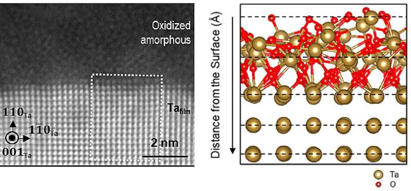
image of a tantalum (Ta) film surface shows an amorphous oxide above the regularly arrayed atoms of crystalline Ta metal. Right: The STEM imaging combined with computational modeling revealed details of the interface between these layers, including the formation of the amorphous oxide (top layer) and a suboxide layer that retains crystalline features (second layer) above the regularly arrayed tantalum atoms. Credit: Brookhaven National Laboratory

Scientists at the U.S. Department of Energy’s (DOE) Brookhaven National Laboratory and DOE’s Pacific Northwest National Laboratory (PNNL) have used a combination of scanning transmission electron microscopy (STEM) and computational modeling to get a closer look and deeper understanding of tantalum oxide. When this amorphous oxide layer forms on the surface of tantalum—a superconductor that shows great promise for making the “qubit” building blocks of a quantum computer—it can impede the material’s ability to retain quantum information.

Learning how the oxide forms may offer clues as to why this happens—and potentially point to ways to prevent quantum coherence loss. The research was recently published in the journal ACS Nano.

The paper builds on earlier research by a team at Brookhaven’s Center for Functional Nanomaterials (CFN), Brookhaven’s National Synchrotron Light Source II (NSLS-II), and Princeton University that was conducted as part of the Co-design Center for Quantum Advantage (C2QA), a Brookhaven-led national quantum information science research center in which Princeton is a key partner.

“In that work, we used X-ray photoemission spectroscopy at NSLS-II to infer details about the type of oxide that forms on the surface of tantalum when it is exposed to oxygen in the air,” said Mingzhao Liu, a CFN scientist and one of the lead authors on the study. “But we wanted to understand more about the chemistry of this very thin layer of oxide by making direct measurements,” he explained.

So, in the new study, the team partnered with scientists in Brookhaven’s Condensed Matter Physics & Materials Science (CMPMS) Department to use advanced STEM techniques that enabled them to study the ultrathin oxide layer directly. They also worked with theorists at PNNL who performed computational modeling that revealed the most likely arrangements and interactions of atoms in the material as they underwent oxidation.

Together, these methods helped the team build an atomic-level understanding of the ordered crystalline lattice of tantalum metal, the amorphous oxide that forms on its surface, and intriguing new details about the interface between these layers.

“The key is to understand the interface between the surface oxide layer and the tantalum film because this interface can profoundly impact qubit performance,” said study co-author Yimei Zhu, a physicist from CMPMS, echoing the wisdom of Nobel laureate Herbert Kroemer, who famously asserted, “The interface is the device.”

Emphasizing that “quantitatively probing a mere one-to-two-atomic-layer-thick interface poses a formidable challenge,” Zhu noted, “we were able to directly measure the atomic structures and bonding states of the oxide layer and tantalum film as well as identify those of the interface using the advanced electron microscopy techniques developed at Brookhaven.”

“The measurements reveal that the interface consists of a ‘suboxide’ layer nestled between the periodically ordered tantalum atoms and the fully disordered amorphous tantalum oxide. Within this suboxide layer, only a few oxygen atoms are integrated into the tantalum crystal lattice,” Zhu said.

The combined structural and chemical measurements offer a crucially detailed perspective on the material. Density functional theory calculations then helped the scientists validate and gain deeper insight into these observations.

“We simulated the effect of gradual surface oxidation by gradually increasing the number of oxygen species at the surface and in the subsurface region,” said Peter Sushko, one of the PNNL theorists.

By assessing the thermodynamic stability, structure, and electronic property changes of the tantalum films during oxidation, the scientists concluded that while the fully oxidized amorphous layer acts as an insulator, the suboxide layer retains features of a metal.

“We always thought if the tantalum is oxidized, it becomes completely amorphous, with no crystalline order at all,” said Liu. “But in the suboxide layer, the tantalum sites are still quite ordered.”

With the presence of both fully oxidized tantalum and a suboxide layer, the scientists wanted to understand which part is most responsible the loss of coherence in qubits made of this superconducting material.

“It’s likely the oxide has multiple roles,” Liu said.

First, he noted, the fully oxidized amorphous layer contains many lattice defects. That is, the locations of the atoms are not well defined. Some atoms can shift around to different configurations, each with a different energy level. Though these shifts are small, each one consumes a tiny bit of electrical energy, which contributes to loss of energy from the qubit.

“This so-called two-level system loss in an amorphous material brings parasitic and irreversible loss to the quantum coherence—the ability of the material to hold onto quantum information,” Liu said.

But because the suboxide layer is still crystalline, “it may not be as bad as people were thinking,” Liu said. Maybe the more fixed atomic arrangements in this layer will minimize two-level system loss.

Then again, he noted, because the suboxide layer has some metallic characteristics, it could cause other problems.

“When you put a normal metal next to a superconductor, that could contribute to breaking up the pairs of electrons that move through the material with no resistance,” he noted. “If the pair breaks into two electrons again, then you will have loss of superconductivity and coherence. And that is not what you want.”

Future studies may reveal more details and strategies for preventing loss of superconductivity and quantum coherence in tantalum.

More information: Junsik Mun et al, Probing Oxidation-Driven Amorphized Surfaces in a Ta(110) Film for Superconducting Qubit, ACS Nano (2023). DOI: 10.1021/acsnano.3c10740

Journal information: ACS Nano 

Provided by Brookhaven National Laboratory