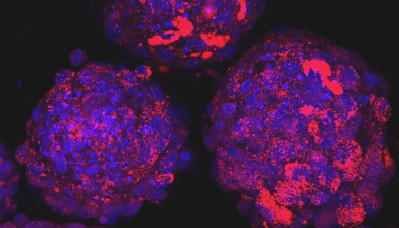
Human mesenchymal stem cells were differentiated into fat cells and the fat vacuoles were stained: stem cells and their differentiation products contain specific fatty sweet surface structures (glycolipids) that help distinguish them from each other. Credit: Institute of Cell and Tissue Culture Technologies, BOKU Vienna
Glycolipids, basically “fatty sweet” molecules, are a relatively unknown group of lipids. A new method developed by an Austrian team led by chemist Evelyn Rampler of the University of Vienna has now provided deeper insights into the functioning of certain glycolipids located on the surfaces of stem cells. The approach presented by the researchers from the University of Vienna, BOKU Vienna and the University of Graz in the open access Journal of the American Chemical Society Au can be applied to a wide range of glycolipid classes.
Pioneering developments in glycoscience for determining the function of sugar structures on cell surfaces recently received recognition with the Nobel Prize in Chemistry awarded to Carolyn Bertozzi. However, research into the class of fatty sweet molecules known as glycolipids is a relatively new, emerging field of study. With their recent work, chemist Evelyn Rampler of the University of Vienna and her colleagues are providing important basic research for this area. Using highly sensitive tools such as mass spectrometry, the structural properties of glycolipids can be investigated.
Decoding of gangliosides
This study aimed at developing a measurement and data analysis method for a specific class of relatively unknown glycolipids, so-called gangliosides, whose composition changes on the cell membrane during stem cell differentiation.
“Previous approaches have not been able to determine the multiple functions of gangliosides in Alzheimer’s disease, dementia or cancer because they lacked the necessary sensitivity. With our new method, we now provide a tool for the comprehensive analysis of gangliosides,” says Evelyn Rampler, group leader at the Institute of Analytical Chemistry at the University of Vienna.
A research consortium of the Medical University Vienna and the University of Vienna will now investigate the relevance of gangliosides and other fatty sweet molecules in cancer. To monitor sugar structures on cells in even greater detail, it would be also possible to combine this new method with the bioorthogonal labeling introduced by Nobel Prize winner Carolyn Bertozzi.
Study of human stem cells
“Our study on human stem cells has shown that the existing patterns of gangliosides change massively depending on which cells or tissues develop from the stem cells. It was therefore possible to identify new markers for different cell types, which now have to be confirmed in independent studies including larger sample sizes,” says Evelyn Rampler.
“Based on our new mass spectrometry method, we were able to measure and describe the molecular diversity of gangliosides in an unprecedented level of detail,” says first author and chemist Katharina Hohenwallner from the University of Vienna.
The study involved experiments with stem cells, carried out by Dominik Egger of the Institute of Cell and Tissue Culture Technologies at BOKU Vienna. In addition, the software “Lipid Data Analyzer” for gangliosides was adapted together with researchers from the University of Graz, Institute of Pharmaceutical Sciences.
Surgical tissue waste as samples
For the analysis, the team used tissue samples derived from medical waste. First, the so-called mesenchymal stem cells were isolated from the tissue and allowed to differentiate into bone, cartilage, and fat cells. In the course of the study, the largest number of gangliosides were identified to date.
Additionally, gangliosides were identified as potential markers to distinguish the different cell types at the chemical level. Based on automated data analysis, the researchers provide a method to comprehensively measure and structurally describe the gangliosides for the first time.
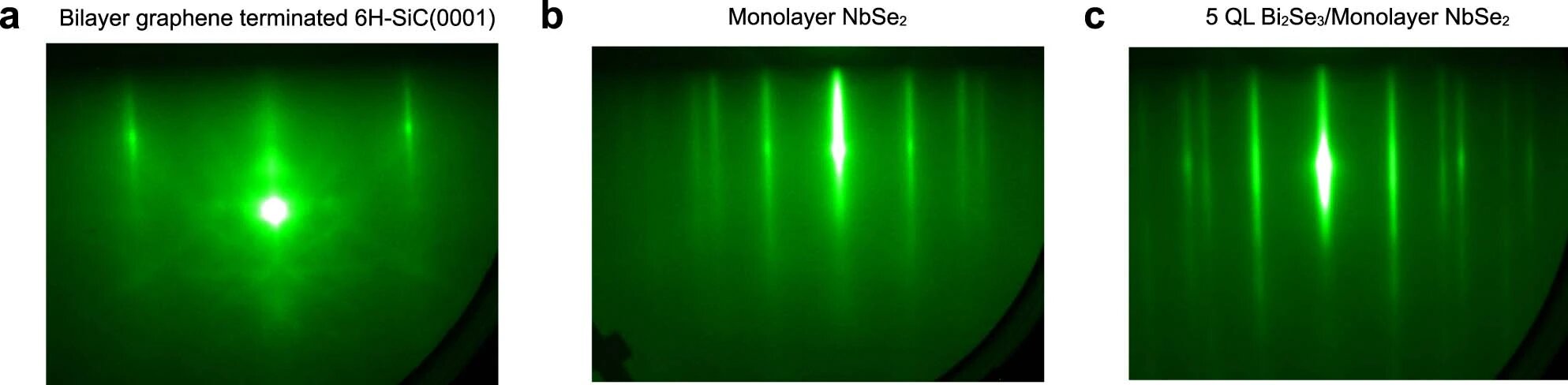
RHEED patterns during MBE growth. (a) Bilayer graphene terminated 6H-SiC(0001) substrate. (b) Monolayer NbSe2 film grown on bilayer graphene. (c) 5 QL Bi2Se3/monolayer NbSe2 heterostructure grown on bilayer graphene. Credit: Nature Materials (2022). DOI: 10.1038/s41563-022-01386-z
A new way to combine two materials with special electrical properties—a monolayer superconductor and a topological insulator—provides the best platform to date to explore an unusual form of superconductivity called topological superconductivity. The combination could provide the basis for topological quantum computers that are more stable than their traditional counterparts.
Superconductors—used in powerful magnets, digital circuits, and imaging devices—allow the electric current to pass without resistance, while topological insulators are thin films only a few atoms thick that restrict the movement of electrons to their edges, which can result in unique properties. A team led by researchers at Penn State describe how they have paired the two materials in a paper appearing Oct. 27 in the journal Nature Materials.
“The future of quantum computing depends on a kind of material that we call a topological superconductor, which can be formed by combining a topological insulator with a superconductor, but the actual process of combining these two materials is challenging,” said Cui-Zu Chang, Henry W. Knerr Early Career Professor and Associate Professor of Physics at Penn State and leader of the research team.
“In this study, we used a technique called molecular beam epitaxy to synthesize both topological insulator and superconductor films and create a two-dimensional heterostructure that is an excellent platform to explore the phenomenon of topological superconductivity.”
In previous experiments to combine the two materials, the superconductivity in thin films usually disappears once a topological insulator layer is grown on top. Physicists have been able to add a topological insulator film onto a three-dimensional “bulk” superconductor and retain the properties of both materials.
However, applications for topological superconductors, such as chips with low power consumption inside quantum computers or smartphones, would need to be two-dimensional.
In this paper, the research team stacked a topological insulator film made of bismuth selenide (Bi2Se3) with different thicknesses on a superconductor film made of monolayer niobium diselenide (NbSe2), resulting in a two-dimensional end-product. By synthesizing the heterostructures at very lower temperature, the team was able to retain both the topological and superconducting properties.
“In superconductors, electrons form ‘Cooper pairs’ and can flow with zero resistance, but a strong magnetic field can break those pairs,” said Hemian Yi, a postdoctoral scholar in the Chang Research Group at Penn State and the first author of the paper.
“The monolayer superconductor film we used is known for its ‘Ising-type superconductivity,’ which means that the Cooper pairs are very robust against the in-plane magnetic fields. We would also expect the topological superconducting phase formed in our heterostructures to be robust in this way.”
By subtly adjusting the thickness of the topological insulator, the researchers found that the heterostructure shifted from Ising-type superconductivity—where the electron spin is perpendicular to the film—to another kind of superconductivity called “Rashba-type superconductivity”—where the electron spin is parallel to the film.
This phenomenon is also observed in the researchers’ theoretical calculations and simulations.
This heterostructure could also be a good platform for the exploration of Majorana fermions, an elusive particle that would be a major contributor to making a topological quantum computer more stable than its predecessors.
“This is an excellent platform for the exploration of topological superconductors, and we are hopeful that we will find evidence of topological superconductivity in our continuing work,” said Chang. “Once we have solid evidence of topological superconductivity and demonstrate Majorana physics, then this type of system could be adapted for quantum computing and other applications.”
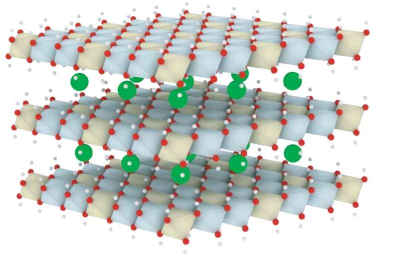
The idealized structure of LDHs. Credit: Mingfei Shao, State Key Laboratory of Chemical Resource Engineering, Beijing University of Chemical Technology, Beijing
To guide the design and synthesis of electrocatalysts toward highly efficient oxygen evolution reactions (OER), researchers from the Beijing University of Chemical Technology have summarized four common strategies to improve the OER performance of layered double hydroxides (LDHs) as well as identifying active sites for LDHs.
They published their work on Sep. 7 in Energy Material Advances.
“With the rising demand and consumption of fossil fuels, energy shortage and environmental pollution are becoming severe and unignorable,” said the corresponding author Mingfei Shao, professor with the State Key Laboratory of Chemical Resource Engineering, Beijing University of Chemical Technology, Beijing. “It is necessary to explore sustainable and renewable energy. Hydrogen, especially, is a new energy with splendid application prospects.”
Production of highly pure hydrogen can be achieved by electrochemical water splitting using the electricity transformed from renewable energies such as wind and solar. But as one of the half reactions, OER is a four-electron process, with a low-efficiency energy utilization, according to Shao.
Shao and his team focus on LDHs, a large type two-dimensional material. The wide tunability, molar ratios and interlayer anions, make it an outstanding catalysts for OER in alkaline medias.
“We summarized four common strategies applied to improve the OER performance of LDHs. Through these strategies, the overpotential of OER can be decreased, leading to a high efficiency of energy utilization,” Shao said. “Some works about the identification of active sites for LDHs are introduced. Revelation of reaction mechanism and active sites provide the theoretical guidance to design efficient electrocatalysts.”
The development and exploration of OER catalysts is mostly in the experimental stage at present, which cannot meet the standards for large-scale practical use. For instance, problems related to enlarging the size of the catalysts and maintaining stability during OER remain. Additionally, most reported preparation methods of LDH-based catalysts are complicated and time-consuming, which results in high costs and restricts their application, according to Shao.
“The recognition of reactive oxygen species such as oxygen species adsorbed by active sites on the surface of electrocatalysts and oxygen radical dispersed in the solution during OER still remains ambiguous due to the instable and unapparent existence of reactive oxygen species,” Shao said. “After recognizing these reactive oxygen species, how to take advantage of them for more efficient OER is still vital.”
“We hope this review can offer ideas to further identify the active sites for LDHs with the purpose of providing guidance to design more advanced electrocatalysts towards electrochemical water splitting,” Shao said.
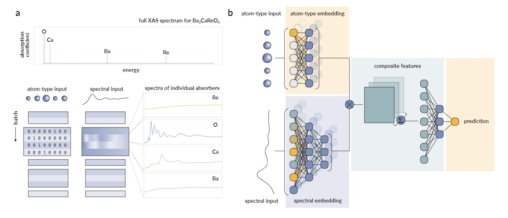
Data structure and model architecture.(a) A schematic of the full XANES spectrum for arepresentative sample in the dataset, showing the signatures from di↵erent absorbing elements on an absolute energyscale. For a given material, the inputs to the NN classifier consist of one-hot encoded atom types (left) and XANESspectra (right) for all absorbing atoms. (b) Schematic of the neural network architecture predicting the (binary)topological class using spectral and atom-type inputs. Spectral and atom-type inputs are individually embedded byfully-connected layers before performing a direct product between corresponding spectral and atomic channels.These composite features are aggregated for a given material and passed to a final fully-connected block to predictthe topological class. Credit: Advanced Materials (2022). DOI: 10.1002/adma.202204113
Topological materials, an exotic class of materials whose surfaces exhibit different electrical or functional properties than their interiors, have been a hot area of research since their experimental realization in 2007—a finding that sparked further research and precipitated a Nobel Prize in Physics in 2016. These materials are thought to have great potential in a variety of fields, and might someday be used in ultraefficient electronic or optical devices, or key components of quantum computers.
But there are many thousands of compounds that may theoretically have topological characteristics, and synthesizing and testing even one such material to determine its topological properties can take months of experiments and analysis. Now a team of researchers at MIT and elsewhere have come up with a new approach that can rapidly screen candidate materials and determine with more than 90 percent accuracy whether they are topological.
Using this new method, the researchers have produced a list candidate materials. A few of these were already known to have topological properties, but the rest are newly predicted by this approach.
The findings are reported in the journal Advanced Materials in a paper by Mingda Li, the Class ’47 Career Development Professor at MIT, graduate students (and twin sisters) Nina Andrejevic at MIT and Jovana Andrejevic at Harvard University, and seven others at MIT, Harvard, Princeton University, and Argonne National Laboratory.
Topological materials are named after a branch of mathematics that describes shapes based on their invariant characteristics, which persist no matter how much an object is continuously stretched or squeezed out of its original shape. Topological materials, similarly, have properties that remain constant despite changes in their conditions, such as external perturbations or impurities.
There are several varieties of topological materials, including semiconductors, conductors, and semimetals, among others. Initially, it was thought that there were only a handful of such materials, but recent theory and calculations have predicted that in fact thousands of different compounds may have at least some topological characteristics. The hard part is figuring out experimentally which compounds may be topological.
Applications for such materials span a wide range, including devices that could perform computational and data storage functions similarly to silicon-based devices but with far less energy loss, or devices to harvest electricity efficiently from waste heat, for example in thermal power plants or in electronic devices. Topological materials can also have superconducting properties, which could potentially be used to build the quantum bits for topological quantum computers.
But all of this relies on developing or discovering the right materials. “To study a topological material, you first have to confirm whether the material is topological or not,” Li says, “and that part is a hard problem to solve in the traditional way.”
A method called density functional theory is used to perform initial calculations, which then need to be followed with complex experiments that require cleaving a piece of the material to atomic-level flatness and probing it with instruments under high-vacuum conditions.
“Most materials cannot even be measured due to various technical difficulties,” Nina Andrejevic says. But for those that can, the process can take a long time. “It’s a really painstaking procedure,” she says.
Sensitivity to spectral energy resolution. The overall recall, precision, and F1 scores for (a) topological and (b) trivial examples as a function of the energy interval E between sampled points of the XANES spectra. Scores are presented for both the SVM and NN models, with scores from the atom-type only models (SVM-type and NN-type) shown as a reference by the dotted lines. Spectra were resampled at lower resolutions by computing their average values over length E intervals along the energy axis for varied E. To maintain the same number of neurons across all resolutions, the averaged values were copied by the number of original samples within each interval such that all spectral inputs have length 200. Credit: Advanced Materials (2022). DOI: 10.1002/adma.202204113
Whereas the traditional approach relies on measuring the material’s photoemissions or tunneling electrons, Li explains, the new technique he and his team developed relies on absorption, specifically, the way the material absorbs X-rays.
Unlike the expensive apparatus needed for the conventional tests, X-ray absorption spectrometers are readily available and can operate at room temperature and atmospheric pressure, with no vacuum needed. Such measurements are widely conducted in biology, chemistry, battery research, and many other applications, but they had not previously been applied to identifying topological quantum materials.
X-ray absorption spectroscopy provides characteristic spectral data from a given sample of material. The next challenge is to interpret that data and how it relates to the topological properties. For that, the team turned to a machine-learning model, feeding in a collection of data on the X-ray absorption spectra of known topological and nontopological materials, and training the model to find the patterns that relate the two. And it did indeed find such correlations.
“Surprisingly, this approach was over 90 percent accurate when tested on more than 1500 known materials,” Nina Andrejevic says, adding that the predictions take only seconds. “This is an exciting result given the complexity of the conventional process.”
Though the model works, as with many results from machine learning, researchers don’t yet know exactly why it works or what the underlying mechanism is that links the X-ray absorption to the topological properties.
“While the learned function relating X-ray spectra to topology is complex, the result may suggest that certain attributes the measurement is sensitive to, such as local atomic structures, are key topological indicators,” Jovana Andrejevic says.
The team has used the model to construct a periodic table that displays the model’s overall accuracy on compounds made from each of the elements. It serves as a tool to help researchers home in on families of compounds that may offer the right characteristics for a given application.
The researchers have also produced a preliminary study of compounds that they have used this X-ray method on, without advance knowledge of their topological status, and compiled a list of 100 promising candidate materials—a few of which were already known to be topological.
“This work represents one of the first uses of machine learning to understand what experiments are trying to tell us about complex materials,” says Joel Moore, the Chern-Simons Professor of Physics at the University of California at Berkeley, who was not associated with this research.
“Many kinds of topological materials are well-understood theoretically in principle, but finding material candidates and verifying that they have the right topology of their bands can be a challenge. Machine learning seems to offer a new way to address this challenge: Even experimental data whose meaning is not immediately obvious to a human can be analyzed by the algorithm, and I am excited to see what new materials will result from this way of looking.”
Anatoly Frenkel, a professor in the Department of Materials Science and Chemical Engineering at Stony Brook University and a senior chemist at Brookhaven National Laboratory, further commented that “it was a really nice idea to consider that the X-ray absorption spectrum may hold a key to the topological character in the measured sample.”
Looking into the HERA tunnel: Berkeley Lab scientists have developed new machine learning algorithms to accelerate the analysis of data collected decades ago by HERA, the world’s most powerful electron-proton collider that ran at the DESY national research center in Germany from 1992 to 2007. Credit: DESY
Protons are tiny yet they carry a lot of heft. They inhabit the center of every atom in the universe and play a critical role in one of the strongest forces in nature.
And yet, protons have a down-to-earth side, too.
Like most particles, protons have spin that act like tiny magnets. Flipping a proton’s spin or polarity may sound like science fiction, but it is the basis of technological breakthroughs that have become essential to our daily lives, such as magnetic resonance imaging (MRI), the invaluable medical diagnostics tool.
Despite such advancements, the proton’s inner workings remain a mystery.
“Basically everything around you exists because of protons—and yet we still don’t understand everything about them. One huge puzzle that physicists want to solve is the proton’s spin,” said Ben Nachman, a physicist who leads the Machine Learning Group in the Physics Division at the Department of Energy’s Lawrence Berkeley National Laboratory (Berkeley Lab).
Understanding how and why protons spin could lead to technological advancements we can’t even imagine today, and help us understand the strong force, a fundamental property that gives all protons and therefore atoms mass.
But it’s not such an easy problem to solve. For one, you can’t exactly pick up a proton and place it in a petri dish: Protons are unfathomably small—their radius is a hair shy of one quadrillionth of a meter, and visible light passes right through them. What’s more, you can’t even observe their insides with the world’s most powerful electron microscopes.
Recent work by Nachman and his team could bring us closer to solving this perplexing proton puzzle.
As a member of the H1 Collaboration—an international group that now includes 150 scientists from 50 institutes and 15 countries, and is based at the DESY national research center in Germany—Nachman has been developing new machine learning algorithms to accelerate the analysis of data collected decades ago by HERA, the world’s most powerful electron-proton collider that ran at DESY from 1992 to 2007.
HERA—a ring 4 miles in circumference—worked like a giant microscope that accelerated both electrons and protons to nearly the speed of light. The particles were collided head-on, which could scatter a proton into its constituent parts: quarks and gluons.
Scientists at HERA took measurements of the particle debris cascading from these electron-proton collisions, what physicists call “deep inelastic scattering,” through sophisticated cameras called particle detectors, one of which was the H1 detector.
Unfolding secrets of the strong force
The H1 stopped collecting data in 2007, the year HERA was decommissioned. Today, the H1 Collaboration is still analyzing the data and publishing results in scientific journals.
The HERA electron-proton collider accelerated both electrons and protons to nearly the speed of light. The particles were collided head-on, which could scatter a proton into its constituent parts: quarks (shown as green and purple balls in the illustration above) and gluons (illustrated as black coils). Credit: DESY
It can take a year or more when using conventional computational techniques to measure quantities related to proton structure and the strong force, such as how many particles are produced when a proton collides with an electron.
And if a researcher wants to examine a different quantity, such as how fast particles are flying in the wake of a quark-gluon jet stream, they would have to start the long computational process all over again, and wait yet another year.
A new machine learning tool called OmniFold—which Nachman co-developed—can simultaneously measure many quantities at once, thereby reducing the amount of time to run an analysis from years to minutes.
OmniFold does this by using neural networks at once to combine computer simulations with data. (A neural network is a machine learning tool that processes complex data that is impossible for scientists to do manually.)
Nachman and his team applied OmniFold to H1 experimental data for the first time in a June issue of the journal Physical Review Letters and more recently at the 2022 Deep Inelastic Scattering (DIS) Conference.
To develop OmniFold and test its robustness against H1 data, Nachman and Vinicius Mikuni, a postdoctoral researcher in the Data and Analytics Services (DAS) group at Berkeley Lab’s National Energy Research Scientific Computing Center (NERSC) and a NERSC Exascale Science Applications Program for Learning fellow, needed a supercomputer with a lot of powerful GPUs (graphics processing units), Nachman said.
Coincidentally, Perlmutter, a new supercomputer designed to support simulation, data analytics, and artificial intelligence experiments requiring multiple GPUs at a time, had just opened up in the summer of 2021 for an “early science phase,” allowing scientists to test the system on real data. (The Perlmutter supercomputer is named for the Berkeley Lab cosmologist and Nobel laureate Saul Perlmutter.)
“Because the Perlmutter supercomputer allowed us to use 128 GPUs simultaneously, we were able to run all the steps of the analysis, from data processing to the derivation of the results, in less than a week instead of months. This improvement allows us to quickly optimize the neural networks we trained and to achieve a more precise result for the observables we measured,” said Mikuni, who is also a member of the H1 Collaboration.
A central task in these measurements is accounting for detector distortions. The H1 detector, like a watchful guard standing sentry at the entrance of a sold-out concert arena, monitors particles as they fly through it. One source of measurement errors happens when particles fly around the detector rather than through it, for example—sort of like a ticketless concert goer jumping over an unmonitored fence rather than entering through the ticketed security gate.
Correcting for all distortions simultaneously had not been possible due to limited computational methods available at the time. “Our understanding of subatomic physics and data analysis techniques have advanced significantly since 2007, and so today, scientists can use new insights to analyze the H1 data,” Nachman said.
Scientists today have a renewed interest in HERA’s particle experiments, as they hope to use the data—and more precise computer simulations informed by tools like OmniFold—to aid in the analysis of results from future electron-proton experiments, such as at the Department of Energy’s next-generation Electron-Ion Collider (EIC).
The EIC—to be built at Brookhaven National Laboratory in partnership with the Thomas Jefferson National Accelerator Facility—will be a powerful and versatile new machine capable of colliding high-energy beams of polarized electrons with a wide range of ions (or charged atoms) across many energies, including polarized protons and some polarized ions.
“It’s exciting to think that our method could one day help scientists answer questions that still remain about the strong force,” Nachman said.
“Even though this work might not lead to practical applications in the near term, understanding the building blocks of nature is why we’re here—to seek the ultimate truth. These are steps to understanding at the most basic level what everything is made of. That is what drives me. If we don’t do the research now, we will never know what exciting new technological advances we’ll get to benefit future societies.”
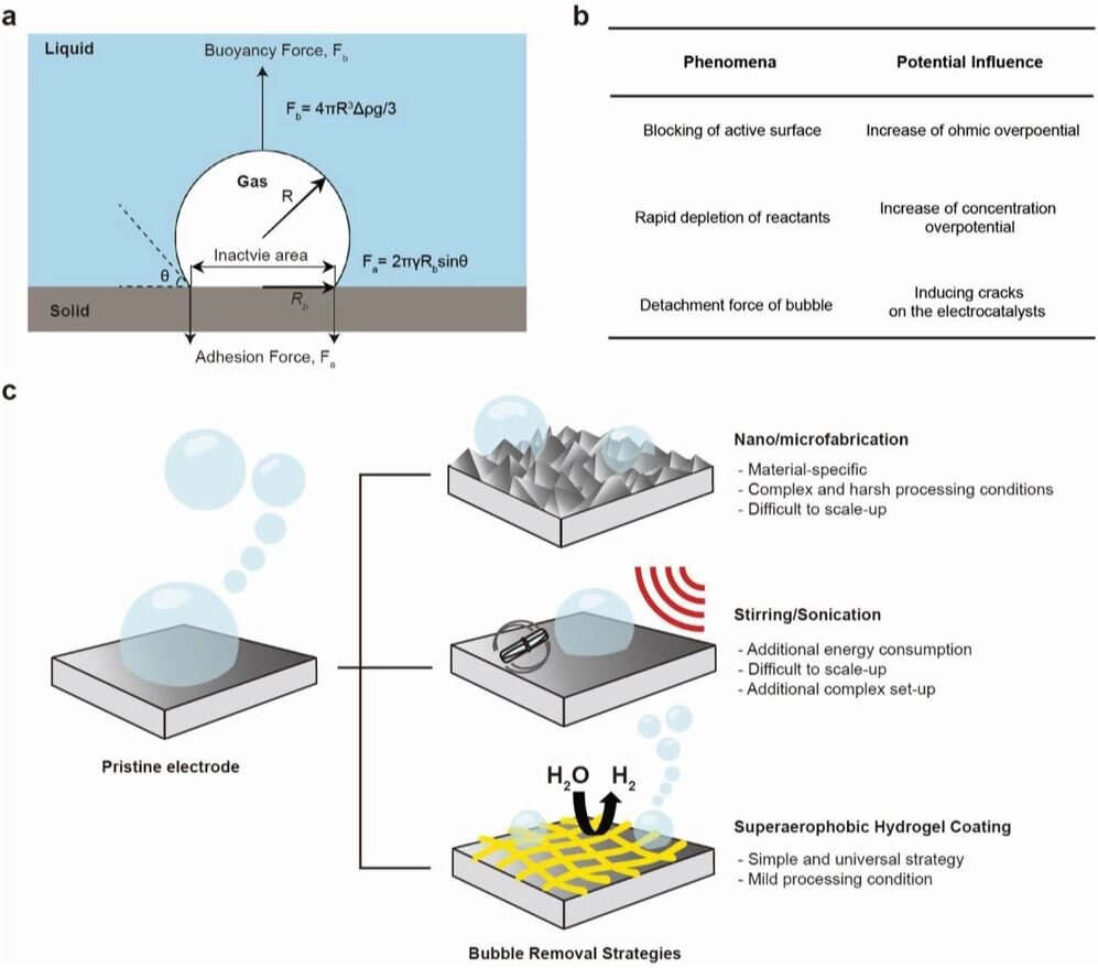
The scheme for a mechanism of bubble-detachment. a) Normal flat electrode, b) the problems of adhered bubbles, and c) various approaches for the removal of gas bubbles. In (a), R, ρ, g, and λ indicate the dimension of bubbles, the density of a solution, gravitational acceleration constant, and surface tension of a solution, respectively. Credit: UNIST
A research team affiliated with UNIST recently reported that the performance of electrodes for an alkaline hydrogen evolution reaction (HER) can be significantly improved even without expensive electrocatalysts and complicated processes by modifying them with superaerophobic polymeric hydrogels. This breakthrough has been led by Professor Jungki Ryu and his research team in the Department of Energy Engineering at UNIST.
In this study, the research team reported a simple strategy to enhance the efficiency of electrochemical hydrogen production by imparting superaerophobicity to an underlying electrode with porous polymeric hydrogels. Superaerophobic hydrogels were readily coated on target substrates by cross-linking polyethyleneimine (PEI) via Schiff-base condensation reactions followed by freeze-drying, noted the research team.
As a result, they could readily control the pore size, porosity, and superaerophobicity of the hydrogel-coated electrodes by varying the concentrations of PEI upon cross-linking. Due to facile removal of as-generated hydrogen bubbles, the NF electrode modified with PEI hydrogel only outperformed those modified with expensive electrocatalysts especially at high current densities, according to the research team.
“We believe that our results can pave the way for the practical application of water electrolysis by providing insights into the design of electrodes and electrolyzers,” noted the research team.
This study has been published in Advanced Energy Materials.
Researchers have discovered a potential new method for making the high-performance magnets used in wind turbines and electric cars without the need for rare earth elements, which are almost exclusively sourced in China.
A team from the University of Cambridge, working with colleagues from Austria, found a new way to make a possible replacement for rare-earth magnets: tetrataenite, a “cosmic magnet” that takes millions of years to develop naturally in meteorites.
Previous attempts to make tetrataenite in the laboratory have relied on impractical, extreme methods. But the addition of a common element—phosphorus—could mean that it’s possible to make tetrataenite artificially and at scale, without any specialized treatment or expensive techniques.
The results are reported in the journal Advanced Science. A patent application on the technology has been filed by Cambridge Enterprise, the University’s commercialization arm, and the Austrian Academy of Sciences.
High-performance magnets are a vital technology for building a zero-carbon economy, and the best permanent magnets currently available contain rare earth elements. Despite their name, rare earths are plentiful in Earth’s crust. However, China has a near monopoly on global production: in 2017, 81% of rare earths worldwide were sourced from China. Other countries, such as Australia, also mine these elements, but as geopolitical tensions with China increase, there are concerns that rare earth supply could be at risk.
“Rare earth deposits exist elsewhere, but the mining operations are highly disruptive: you have to extract a huge amount of material to get a small volume of rare earths,” said Professor Lindsay Greer from Cambridge’s Department of Materials Science & Metallurgy, who led the research. “Between the environmental impacts, and the heavy reliance on China, there’s been an urgent search for alternative materials that do not require rare earths.”
Tetrataenite, an iron-nickel alloy with a particular ordered atomic structure, is one of the most promising of those alternatives. Tetrataenite forms over millions of years as a meteorite slowly cools, giving the iron and nickel atoms enough time to order themselves into a particular stacking sequence within the crystalline structure, ultimately resulting in a material with magnetic properties approaching those of rare-earth magnets.
In the 1960s, scientists were able to artificially form tetrataenite by bombarding iron-nickel alloys with neutrons, enabling the atoms to form the desired ordered stacking, but this technique is not suitable for mass production.
“Since then, scientists have been fascinated with getting that ordered structure, but it’s always felt like something that was very far away,” said Greer. Despite many attempts over the years, it has not yet been possible to make tetrataenite on anything approaching an industrial scale.
Now, Greer and his colleagues from the Austrian Academy of Sciences and the Montanuniversität in Leoben, have found a possible alternative that doesn’t require millions of years of cooling or neutron irradiation.
The team were studying the mechanical properties of iron-nickel alloys containing small amounts of phosphorus, an element that is also present in meteorites. The pattern of phases inside these materials showed the expected tree-like growth structure called dendrites.
“For most people, it would have ended there: nothing interesting to see in the dendrites, but when I looked closer, I saw an interesting diffraction pattern indicating an ordered atomic structure,” said first author Dr. Yurii Ivanov, who completed the work while at Cambridge and is now based at the Italian Institute of Technology in Genoa.
At first glance, the diffraction pattern of tetrataenite looks like that of the structure expected for iron-nickel alloys, namely a disordered crystal not of interest as a high-performance magnet. It took Ivanov’s closer look to identify the tetrataenite, but even so Greer says it’s strange that no one noticed it before.
The researchers say that phosphorus, which is present in meteorites, allows the iron and nickel atoms to move faster, enabling them to form the necessary ordered stacking without waiting for millions of years. By mixing iron, nickel and phosphorus in the right quantities, they were able to speed up tetrataenite formation by between 11 and 15 orders of magnitude, such that it forms over a few seconds in simple casting.
“What was so astonishing was that no special treatment was needed: we just melted the alloy, poured it into a mold, and we had tetrataenite,” said Greer. “The previous view in the field was that you couldn’t get tetrataenite unless you did something extreme, because otherwise you’d have to wait millions of years for it to form. This result represents a total change in how we think about this material.”
While the researchers have found a promising method to produce tetrataenite, more work is needed to determine whether it will be suitable for high-performance magnets. The team are hoping to work on this with major magnet manufacturers.
The work may also force a revision of views on whether the formation of tetrataenite in meteorites really does take millions of years.
In a study that confirms its promise as the next-generation semiconductor material, UC Santa Barbara researchers have directly visualized the photocarrier transport properties of cubic boron arsenide single crystals.
“We were able to visualize how the charge moves in our sample,” said Bolin Liao, an assistant professor of mechanical engineering in the College of Engineering. Using the only scanning ultrafast electron microscopy (SUEM) setup in operation at a U.S. university, he and his team were able to make “movies” of the generation and transport processes of a photoexcited charge in this relatively little-studied III-V semiconductor material, which has recently been recognized as having extraordinary electrical and thermal properties. In the process, they found another beneficial property that adds to the material’s potential as the next great semiconductor.
Their research, conducted in collaboration with physics professor Zhifeng Ren’s group at the University of Houston, who specialize in fabricating high-quality single crystals of cubic boron arsenide, appears in the journal Matter.
‘Ringing the bell’
Boron arsenide is being eyed as a potential candidate to replace silicon, the computer world’s staple semiconductor material, due to its promising performance. For one thing, with an improved charge mobility over silicon, it easily conducts current (electrons and their positively charged counterpart, “holes”). However, unlike silicon, it also conducts heat with ease.
“This material actually has 10 times higher thermal conductivity than silicon,” Liao said. This heat conducting—and releasing—ability is particularly important as electronic components become smaller and more densely packed, and pooled heat threatens the devices’ performance, he explained.
“As your cellphones become more powerful, you want to be able to dissipate the heat, otherwise you have efficiency and safety issues,” he said. “Thermal management has been a challenge for a lot of microelectronic devices.”
What gives rise to the high thermal conductivity of this material, it turns out, can also lead to interesting transport properties of photocarriers, which are the charges excited by light, for example, in a solar cell. If experimentally verified, this would indicate that cubic boron arsenide can also be a promising material for photovoltaic and light detection applications. Direct measurement of photocarrier transport in cubic boron arsenide, however, has been challenging due to the small size of available high-quality samples.
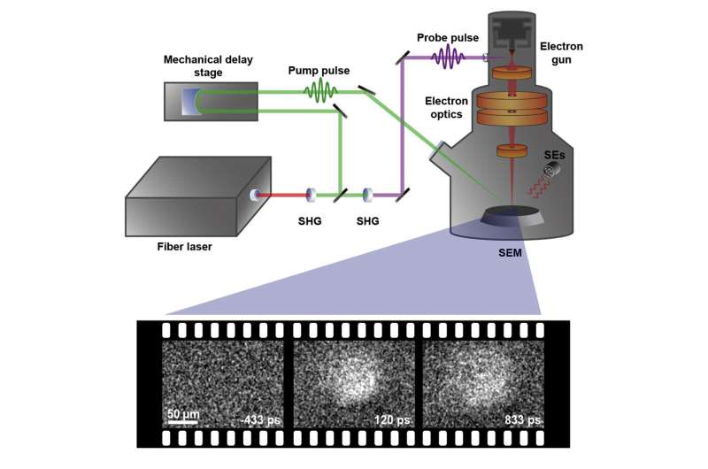
The research team’s study combines two feats: The crystal growth skills of the University of Houston team, and the imaging prowess at UC Santa Barbara. Combining the abilities of the scanning electron microscope and femtosecond ultrafast lasers, the UCSB team built what is essentially an extremely fast, exceptionally high-resolution camera.
“Electron microscopes have very good spatial resolution—they can resolve single atoms with their sub-nanometer spatial resolution—but they’re typically very slow,” Liao said, noting this makes them excellent for capturing static images.
“With our technique, we couple this very high spatial resolution with an ultrafast laser, which acts as a very fast shutter, for extremely high time resolution,” Liao continued. “We’re talking about one picosecond—a millionth of a millionth of a second. So we can make movies of these microscopic energy and charge transport processes.” Originally invented at Caltech, the method was further developed and improved at UCSB from scratch and now is the only operational SUEM setup at an American university.
“What happens is that we have one pulse of this laser that excites the sample,” explained graduate student researcher Usama Choudhry, the lead author of the Matter paper. “You can think of it like ringing a bell; it’s a loud noise that slowly diminishes over time.” As they “ring the bell,” he explained, a second laser pulse is focused onto a photocathode (“electron gun”) to generate a short electron pulse to image the sample. They then scan the electron pulse over time to gain a full picture of the ring. “Just by taking a lot of these scans, you can get a movie of how the electrons and holes get excited and eventually go back to normal,” he said.
Among the things they observed while exciting their sample and watching the electrons return to their original state is how long the “hot” electrons persist.
“We found, surprisingly, the ‘hot’ electrons excited by light in this material can persist for much longer times than in conventional semiconductors,” Liao said. These “hot” carriers were seen to persist for more that 200 picoseconds, a property that is related to the same feature that is responsible for the material’s high thermal conductivity. This ability to host “hot” electrons for significantly longer amounts of time has important implications.
“For example, when you excite the electrons in a typical solar cell with light, not every electron has the same amount of energy,” Choudhry explained. “The high-energy electrons have a very short lifetime, and the low-energy electrons have a very long lifetime.” When it comes to harvesting the energy from a typical solar cell, he continued, only the low-energy electrons are efficiently being collected; the high-energy ones tend to lose their energy rapidly as heat. Because of the persistence of the high-energy carriers, if this material was used as a solar cell, more energy could efficiently be harvested from it.
With boron arsenide beating silicon in three relevant areas—charge mobility, thermal conductivity and hot photocarrier transport time—it has the potential to become the electronics world’s next state-of-the-art material. However, it still faces significant hurdles—fabrication of high-quality crystals in large quantities—before it can compete with silicon, enormous amounts of which can be manufactured relatively cheaply and with high quality. But Liao doesn’t see too much of a problem.
“Silicon is now routinely available because of years of investment; people started developing silicon around the 1930s and ’40s,” he said. “I think once people recognize the potential of this material, there will be more effort put into finding ways to grow and use it. UCSB is actually uniquely positioned for this challenge with strong expertise in semiconductor development.”
Illustration of yeast cells during the illumination with blue light. Credit: Max-Planck-Institut für Biochemie
Neurodegenerative diseases like Alzheimer’s, Parkinson’s or Huntington’s disease are characterized by the deposition of protein clumps, so-called protein aggregates, in the brains of patients. Even though disease-relevant proteins—such as the huntingtin protein in Huntington’s disease—are present in all cells of the human brain, aggregates of huntingtin form in a specific region of the brain during the initial stage of the disease.
A recent study by the group of Ulrich Hartl from the Max Planck Institute of Biochemistry investigates the influence, that the cell type has on this preference of aggregate formation in a distinct brain region. The study has been published in the scientific journal Molecular Cell. To address this phenomenon, the researchers performed experiments in a yeast model system.
Artificial protein aggregation through blue light illumination
Similar to the human brain, the formation of huntingtin aggregates in yeast also depend on the cell type, the so-called yeast strain. While the huntingtin protein forms aggregates in some yeast strains, it remains soluble in others. Why this is the case hasn’t been understood so far.
To investigate the distinction between different yeast strains and how they contribute to the formation of huntingtin aggregates, the researchers utilized recent advances in the field of optogenetics. They biotechnologically manipulated yeast strains that normally do not allow the aggregation of huntingtin and integrated a molecular switch that could be activated with blue light. This way, huntingtin aggregates could be formed simply by illuminating the cells with blue light.
Comparing the yeast cells that naturally form huntingtin aggregates with those, that only do so after their activation with blue light, caught the researchers by surprise. Only in cells where huntingtin aggregates already form naturally, but not in those where the aggregation of huntingtin was artificially induced with blue light, were toxic effects observed.
The first author of the study, Michael Gropp, reasoned that this phenomenon came about because smaller intermediates, rather than large aggregates, are the actual toxic version of the protein. Only in yeast cells that form huntingtin aggregates naturally, do these smaller toxic intermediates, the oligomers, exist. Here, large aggregates arise slowly, through the accumulation of proteins around the smaller intermediates.
These small intermediates are bypassed when the aggregation of huntingtin is induced artificially with blue light. Large aggregates then appear much more rapidly, avoiding toxic effects.
The role of prions during aggregate formation
But why do some yeast strains form huntingtin aggregates, while other genetically identical strains do not? Further assays in yeast and experiments with purified proteins—proteins that were artificially enriched in a test tube—helped the researchers to understand this phenomenon. Some yeast strains naturally contain protein aggregates of certain proteins, the prions.
These prion aggregates are not harmful for the cells. However, due to their specific structure, these prion aggregates can influence soluble huntingtin proteins and impose their structure on them. As a result, soluble huntingtin proteins convert into an aggregated state. A side effect of this process is the appearance of toxic intermediates. Yeast strains that naturally do not form huntingtin aggregates also do not possess prions and are therefore unable to generate toxic intermediates, despite the artificial induction of large huntingtin aggregates with blue light.
Possible implications for human disease
In recent years, many human proteins have been characterized that share similarities with the prions in yeast. A bioinformatic analysis of previously published data sets from mouse models and human cell cultures showed that mammalian proteins with such prion-like characteristics preferentially accumulate in neurons.
With the increasing age of an individual, they tend to form aggregates. The authors of the study suspect that the aggregates of these prion-like proteins can in turn force the aggregation of disease-relevant proteins, such as huntingtin, in certain brain areas and thus contribute to the disease progression in neurodegenerative disorders. Further investigation of this hypothesis is still ongoing.
An international group of researchers from Technical University of Denmark (DTU) and Chalmers University of Technology in Gothenburg, Sweden have achieved dizzying data transmission speeds and are the first in the world to transmit more than 1 petabit per second (Pbit/s) using only a single laser and a single optical chip.
1 petabit corresponds to 1 million gigabits.
In the experiment, the researchers succeeded in transmitting 1.8 Pbit/s, which corresponds to twice the total global Internet traffic. And only carried by the light from one optical source. The light source is a custom-designed optical chip, which can use the light from a single infrared laser to create a rainbow spectrum of many colors, i.e., many frequencies. Thus, the one frequency (color) of a single laser can be multiplied into hundreds of frequencies (colors) in a single chip.
All the colors are fixed at a specific frequency distance from each other—just like the teeth on a comb—which is why it is called a frequency comb. Each color (or frequency) can then be isolated and used to imprint data. The frequencies can then be reassembled and sent over an optical fiber, thus transmitting data. Even a huge volume of data, as the researchers have discovered.
One single laser can replace thousands
The experimental demonstration showed that a single chip could easily carry 1.8 Pbit/s, which—with contemporary state-of-the-art commercial equipment—would otherwise require more than 1,000 lasers.
Victor Torres Company, professor at Chalmers University of Technology, is head of the research group that has developed and manufactured the chip.
“What is special about this chip is that it produces a frequency comb with ideal characteristics for fiber-optical communications—it has high optical power and covers a broad bandwidth within the spectral region that is interesting for advanced optical communications,” says Victor Torres Company.
Interestingly enough, the chip was not optimized for this particular application.
“In fact, some of the characteristic parameters were achieved by coincidence and not by design,” says Victor Torres Company. “However, with efforts in my team, we are now capable to reverse engineer the process and achieve with high reproducibility microcombs for target applications in telecommunications.”
Enormous potential for scaling
In addition, the researchers created a computational model to examine theoretically the fundamental potential for data transmission with a single chip identical to the one used in the experiment. The calculations showed enormous potential for scaling up the solution.
Professor Leif Katsuo Oxenløwe, Head of the Center of Excellence for Silicon Photonics for Optical Communications (SPOC) at DTU, says:
“Our calculations show that—with the single chip made by Chalmers University of Technology, and a single laser—we will be able to transmit up to 100 Pbit/s. The reason for this is that our solution is scalable—both in terms of creating many frequencies and in terms of splitting the frequency comb into many spatial copies and then optically amplifying them, and using them as parallel sources with which we can transmit data. Although the comb copies must be amplified, we do not lose the qualities of the comb, which we utilize for spectrally efficient data transmission.”
This is how you pack light with data
Packing light with data is known as modulation. Here, the wave properties of light are utilized such as:
Amplitude (the height/strength of the waves)
Phase (the “rhythm” of the waves, where it is possible to make a shift so that a wave arrives either a little earlier or a little later than expected)
Polarization (the directions in which the waves spread).
By changing these properties, you create signals. The signals can be translated into either ones or zeros—and thus utilized as data signals.
Reduces Internet power consumption
The researchers’ solution bodes well for the future power consumption of the Internet.
“In other words, our solution provides a potential for replacing hundreds of thousands of the lasers located at Internet hubs and data centers, all of which guzzle power and generate heat. We have an opportunity to contribute to achieving an Internet that leaves a smaller climate footprint,” says Leif Katsuo Oxenløwe.
Even though the researchers have broken the petabit barrier for a single laser source and a single chip in their demonstration, there is still some development work ahead before the solution can be implemented in our current communication systems, according to Leif Katsuo Oxenløwe.
“All over the world, work is being done to integrate the laser source in the optical chip, and we’re working on that as well. The more components we can integrate in the chip, the more efficient the whole transmitter will be, i.e., laser, comb-creating chip, data modulators, and any amplifier elements. It will be an extremely efficient optical transmitter of data signals,” says Leif Katsuo Oxenløwe.